DocID13284 Rev 2 389/564
UM0404 Analog / digital converter
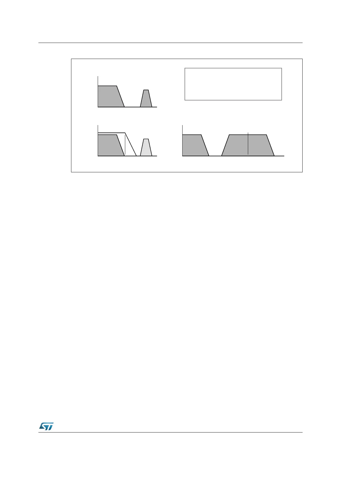
Figure 167. Anti-aliasing filter and conversion rate
The considerations above lead to impose new constraints to the external circuit, to reduce
the accuracy error due to the voltage drop on C
S
; from the two charge balance equations
above, it is simple to derive the following relation between the ideal and real sampled
voltage on C
S
:
From this formula, in the worst case (when V
A
is maximum, that is for instance 5V),
assuming to accept a maximum error of half a count (~2.44mV), it is immediately evident a
constraints on C
F
value:
In the next section an example of how to design the external network is provided, assuming
some reasonable values for the internal parameters and making hypothesis on the
characteristics of the analog signal to be sampled.
f
0
f
Analog Source Bandwidth (V
A
)
f
0
f
Sampled Signal Spectrum (f
C
= Conversion Rate)
f
C
f
Anti-Aliasing Filter (f
F
= RC Filter pole)
f
F
2 f
0
≤ f
C
(Nyquist)
f
F
= f
0
(Anti-aliasing Filtering Condition)
T
C
≤ 2 R
F
C
F
(Conversion Rate vs. Filter Pole)
Noise
V
A
V
A2
------------
C
P1
C
P2
+C
F
+
C
P1
C
P2
+C
F
C
S
++
-----------------------------------------------
=