DocID13284 Rev 2 217/564
UM0404 The general purpose timer units
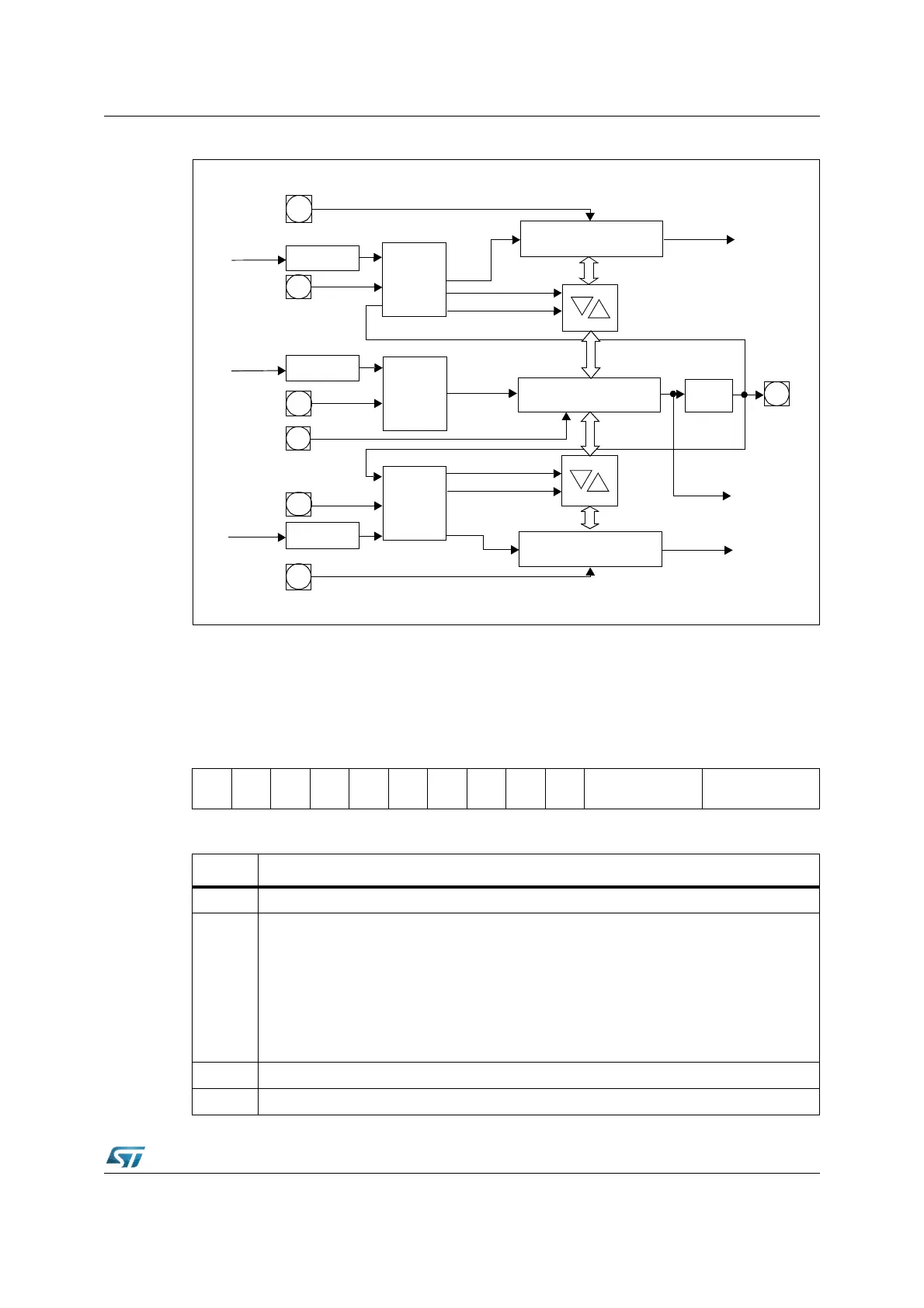
Figure 76. GPT1 block diagram
9.1.1 GPT1 core timer T3
The core timer T3 is configured and controlled via its bit-addressable control register
T3CON.
T3CON (FF42h / A1h) SFR Reset Value: 0000h
2
n
n=3...10
2
n
n=3...10
2
n
n=3...10
T2EUD
T2IN
CPU Clock
CPU Clock
CPU Clock
T3EUD
T4IN
T3IN
T4EUD
T2
Mode
T3
Mode
T4
Mode
GPT1 Timer T2
GPT1 Timer T3
GPT1 Timer T4
T3OTL
Reload
Capture
U/D
U/D
Reload
Capture
Interrupt
Request
Interrupt
Request
Interrupt
Request
T3OUT
U/D
P5.15
P3.7
P3.6
P3.4
P3.5
P5.14
P3.3
1514131211109876543210
-----
T3OT
L
T3OE
T3UD
E
T3UD T3R T3M T3I
RW RW RW RW RW RW RW RW RW RW RW
Bit Function
T3I Timer 3 Input Selection - Depends on the operating mode, see respective sections.
T3M
Timer 3 Mode Control (Basic Operating Mode)
0 0 0: Timer Mode
0 0 1: Counter Mode
0 1 0: Gated Timer with Gate active low
0 1 1: Gated Timer with Gate active high
1 0 X: Reserved (do not use this combination)
1 1 0: Incremental interface mode
1 1 1: Reserved (do not use this combination)
T3R Timer 3 Run bit: T3R = ‘0’: Timer / Counter 3 stops - T3R = ‘1’: Timer / Counter 3 runs
T3UD Timer 3 Up / Down Control
(1)