DocID13284 Rev 2 191/564
UM0404 The external bus interface
cycle refers to the same CLKOUT edges as usual (the data transfer is delayed by one CPU
clock cycle). This allows more time for the address to be latched.
Note: ALECTL0 is ‘1’ after reset to select the slowest possible bus cycle, the other ALECTLx are
‘0’ after reset.
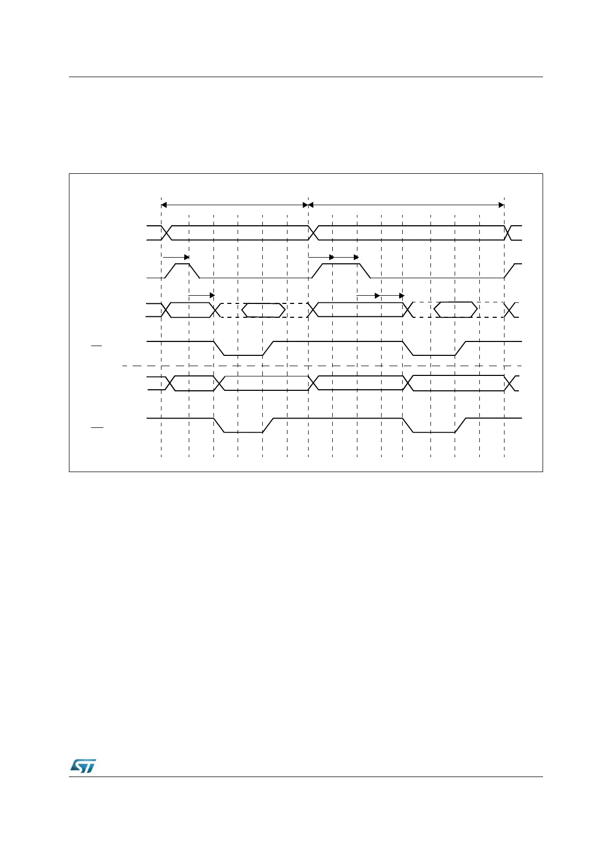
Figure 62. ALE length control
8.3.2 Programmable memory cycle time
The ST10F276 allows the user to adjust the controller's external bus cycles to the access
time of the respective memory or peripheral. This access time is the total time required to
move the data to the destination. It represents the period of time during which the
controller’s signals do not change.
The external bus cycles of the ST10F276 can be extended for a memory or a peripheral
which cannot keep pace with the controller’s maximum speed: some wait-states are
introduced during the access (see Figure 63). During these memory cycle time wait-states,
the CPU is idle, if this access is required for the execution of the current instruction. The
memory cycle time wait-states can be programmed in increments of one CPU clock within a
range from 0 to 15 (default after reset) via the MCTC fields of the BUSCON registers. 15-
[MCTC] wait-states will be inserted.
Segment (P4)
ALE
BUS (P0)
RD
BUS (P0)
WR
Normal Multiplexed Bus Cycle
Lengthened Multiplexed Bus Cycle
Address Address
Address Data/Instr. Address Data/Instr.
Data
1 Setup
2 Hold
1 Setup
2 Hold
AddressDataAddress