Parallel ports UM0404
146/564 DocID13284 Rev 2
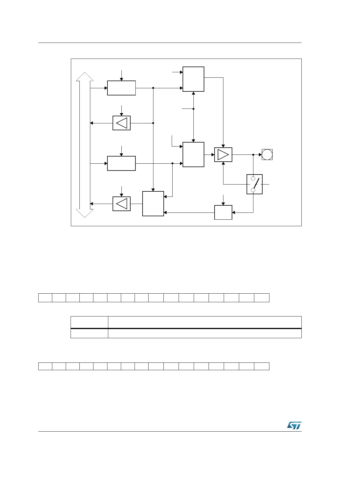
Figure 32. Block diagram of a PORT1 pin
6.4 Port2
If this 16-bit port is used for general purpose I/O, the direction of each line can be configured
via the corresponding direction register DP2. Each port line can be switched into push-pull
or open drain mode via the open drain control register ODP2.
P2 (FFC0h / E0h) SFR Reset Value: 0000h
DP2 (FFC2h / E1h) SFR Reset Value: 0000h
Direction
Latch
Write DP1H.y / DP1L.y
Read DP1H.y / DP1L.y
Port Output
Latch
Write P1H.y / P1L.y
Read P1H.y / P1L.y
Internal Bus
MUX
0
1
MUX
0
1
MUX
0
1
“1”
Input
Latch
Clock
P1H.y
P1L.y
Output
Buffer
y = 7...0
Alternate
Function
Enable
Port Data
Output
Alternate
Data
Output
XP1DIDIS.y
1514131211109876543210
P2.15P2.14P2.13P2.12P2.11P2.10 P2.9 P2.8 P2.7 P2.6 P2.5 P2.4 P2.3 P2.2 P2.1 P2.0
RW RW RW RW RW RW RW RW RW RW RW RW RW RW RW RW
Bit Function
P2.y Port data register P2 bit y
1514131211109876543210
DP2.15 DP2.14DP2.13 DP2.12 DP2.11DP2.10 DP2.9 DP2.8 DP2.7 DP2.6 DP2.5 DP2.4 DP2.3 DP2.2 DP2.1 DP2.0
RW RW RW RW RW RW RW RW RW RW RW RW RW RW RW RW