The external bus interface UM0404
202/564 DocID13284 Rev 2
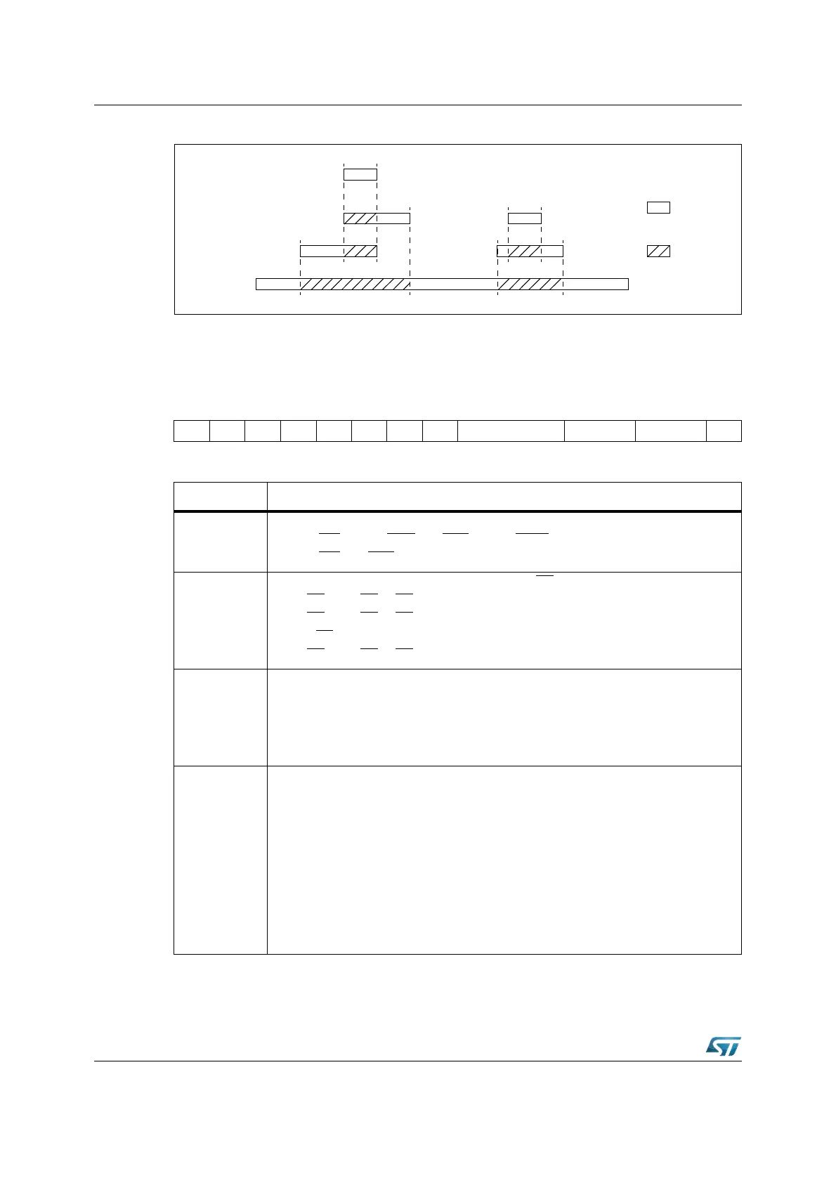
Figure 68. Address window arbitration
Note: Only the indicated overlaps are defined. All other overlaps lead to erroneous bus cycles.
ADDRSEL4 may not overlap ADDRSEL2 or ADDRSEL1. The hard-wired (or
programmable) XADRSx registers are defined non-overlapping.
RP0H (F108h / 84h) SFR Reset Value: - - xxh
Active
Window
Inactive
Window
BUSCON0
BUSCON1
BUSCON2
XBCONx
BUSCON3
BUSCON4
1514131211109876543210
-------- CLKCFG SALSEL CSSEL WRC
RRRR
Bit Function
WRC
(1)
1. These bits are set according to Port0 configuration during any reset sequence.
Write Configuration Control (Set according to pin P0H.0 during reset)
‘0’: Pins WR
acts as WRL, pin BHE acts as WRH.
‘1’: Pins WR and BHE retain their normal function.
CSSEL
(1)
Chip Select Line Selection (Number of active CS outputs)
0 0: 3 CS lines: CS2...CS0
0 1: 2 CS lines: CS1...CS0
1 0: No CS
lines at all
1 1: 5 CS lines: CS4...CS0 (Default without pull-downs)
SALSEL
(1)
Segment Address Line Selection (Number of active segment address outputs)
0 0: 4-bit segment address: A19...A16
0 1: No segment address lines at all
1 0: 8-bit segment address: A23...A16
1 1: 2-bit segment address: A17...A16 (Default without pull-downs on P0)
CLKCFG
(1), (2)
2. RP0H.[7...0] bits are loaded only during a long hardware reset.
P0H.7-5
111
110
101
100
011
010
001
000
CPU Frequency
f
CPU
= f
XTAL
x F
f
XTAL
x 4
f
XTAL
x 3
f
XTAL
x 8
f
XTAL
x 5
f
XTAL
x 1
f
XTAL
x 10
f
XTAL
x 0.5
f
XTAL
x 16
Notes
Default configuration without pull-downs on P0
Direct drive
(3)
CPU clock via prescaler
(3)
3. Refer to datasheet for more details about input clock ranges.