DocID13284 Rev 2 145/564
UM0404 Parallel ports
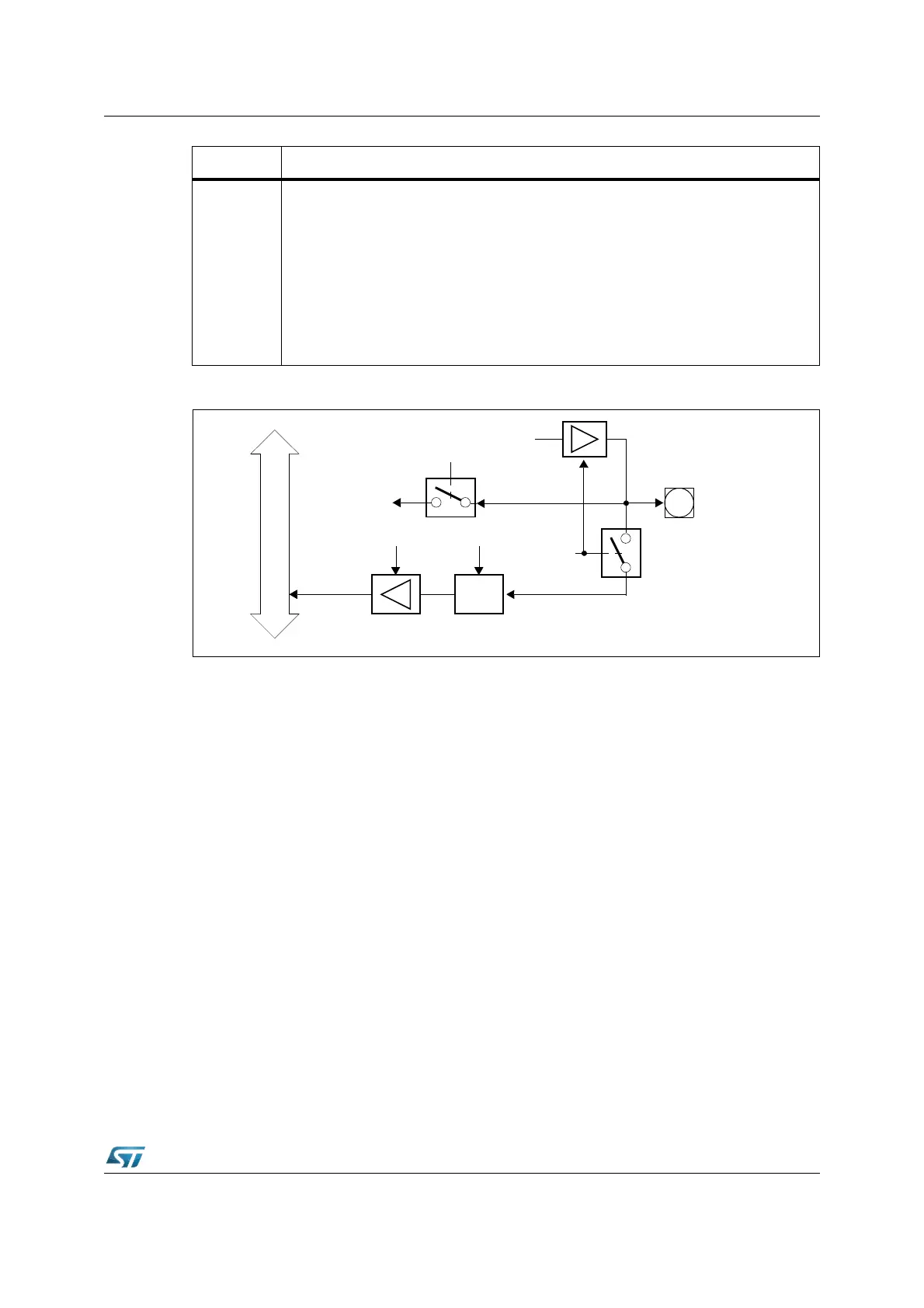
Figure 31. Block diagram of input section of a P1L pin
Bit Function
XP1DIDIS.y
PORT1 Digital Disable register bit y
‘0’: Port line P1.y digital input and output are not disabled: the port pin is defined
through the corresponding bits of the standard registers P1L/DP1L. General Purpose
Input/Output functionality is available, and also external memory interface
functionality.
‘1’: Port line P1.y digital input and output are disabled (necessary for input leakage
current reduction and to avoid undesired conflict between output driver configuration
and analog input signal). Once this bit is set, P1L/DP1L corresponding bits are no
longer effective and the external memory interface functionality is masked on the
single bit.
Read Port P1L.x
Internal Bus
Input
Latch
Clock
P1L.x/ANy
Read
Buffer
to Sample + Hold
Circuit
Channel
Select
Analog
Switch
x = 7...0
XP1DIDIS.x
y = 23 ...16