DocID13284 Rev 2 341/564
UM0404 The capture / compare units
match was detected, the compare register is reloaded with a new value, this value will not
become effective until the next timer period.
In order to use the respective port pin as compare signal output pin CCxIO for compare
register CCx in compare mode 3 this port pin must be configured as output and the
corresponding direction control bit must be set to ‘1’. With this configuration, the initial state
of the output signal can be programmed or its state can be modified at any time by writing to
the port output latch.
In compare mode 3 the port latch is set upon a compare event and cleared upon a timer
overflow (see Figure 141).
However, when compare value and reload value for a channel are equal the respective
interrupt requests will be generated, only the output signal is not changed (set and clear
would coincide in this case).
Note: If the port output latch is written to by software at the same time it would be altered by a
compare event, the software write will have priority. In this case the hardware-triggered
change will not become effective.
On channels 24...27 compare mode 1 will generate interrupt requests but no output function
is provided.
16.5.5 Double register compare mode
In double-register compare mode two compare registers work together to control one output
pin. This mode is selected by a special combination of modes for these two registers.
For double-register mode the 16 capture / compare registers of each CAPCOM unit are
regarded as two banks of 8 registers each. Registers CC0...CC7 and CC16...CC23 form
bank 1 while registers CC8...CC15 and CC24...CC31 form bank 2 (respectively). For
double-register mode a bank 1 register and a bank 2 register form a register pair. Both
registers of this register pair operate on the pin associated with the bank 1 register (pins
CC0IO...CC7IO and CC16IO...CC23IO).
The relationship between the bank 1 and bank 2 register of a pair and the effected output
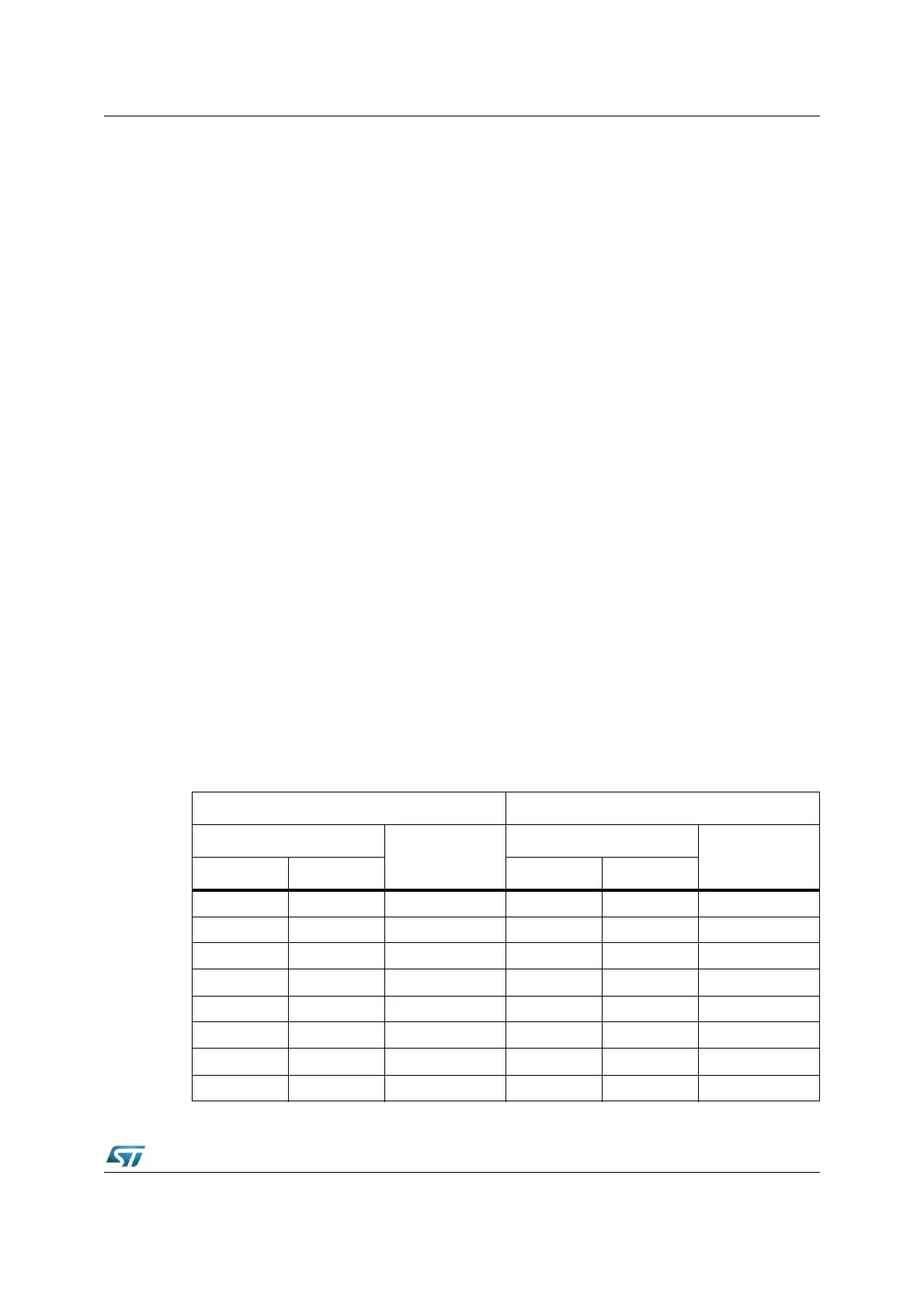
pins for double-register compare mode is listed in the Table 50.
Table 50. Register pairs for double-register compare mode
CAPCOM1 unit CAPCOM2 unit
Register pair
Associated
output pin
Register pair
Associated
output pin
Bank 1 Bank 2 Bank 1 Bank 2
CC0 CC8 CC0IO CC16 CC24 CC16IO
CC1 CC9 CC1IO CC17 CC25 CC17IO
CC2 CC10 CC2IO CC18 CC26 CC18IO
CC3 CC11 CC3IO CC19 CC27 CC19IO
CC4 CC12 CC4IO CC20 CC28 CC20IO
CC5 CC13 CC5IO CC21 CC29 CC21IO
CC6 CC14 CC6IO CC22 CC30 CC22IO
CC7 CC15 CC7IO CC23 CC31 CC23IO