DocID13284 Rev 2 189/564
UM0404 The external bus interface
Address chip select signals remain active until an access to another address window. An
address chip select becomes active with the falling edge of ALE and becomes inactive with
the falling edge of ALE of an external bus cycle that accesses a different address area. No
spikes will be generated on the chip select lines.
Read or write chip select signals remain active only as long as the associated control
signal (RD
or WR) is active.
This also includes the programmable read/write delay. Read chip select is only activated for
read cycles, write chip select is only activated for write cycles, read/write chip select is
activated for both read and write cycles (write cycles are assumed, if any of the signals
WRH
or WRL becomes active).
These modes save external glue logic, when accessing external devices like latches or
drivers that only provide a single enable input.
Note: CS0
provides an address chip select directly after reset (except for single chip mode) when
the first instruction is fetched.
Internal pull-up devices hold all CS
lines high during reset. After the end of a reset sequence
the pull-up devices are switched off and the pin drivers control the pin levels on the selected
CS
lines. Not selected CS lines will enter the high-impedance state and are available for
general purpose I/O.
The pull-up devices are also active during bus hold on the selected CS
lines, while HLDA is
active and the respective pin is switched to push-pull mode. Open drain outputs will float
during bus hold. In this case external pull-up devices are required or the new bus master is
responsible for driving appropriate levels on the CS
lines.
8.2.8 Segment address versus chip select
The external bus interface supports many configurations for the external memory. By
increasing the number of segment address lines, a linear address space of 256 Kbytes, 1
Mbyte or 16 Mbytes can be addressed.
It is possible to implement a large memory area and to access a great number of external
devices using an external decoder. By increasing the number of CS
lines, accesses can be
made to memory banks or peripherals without external glue logic.
These two features may be combined to optimize the overall system performance. Enabling
4 segment address lines and 5 chip select lines to give access to five memory banks of
1 Mbyte each, so the available address space is 5 Mbytes (without glue logic).
Note: Bit SGTDIS of register SYSCON defines whether the CSP register is saved during interrupt
entry (segmentation active) or not (segmentation disabled).
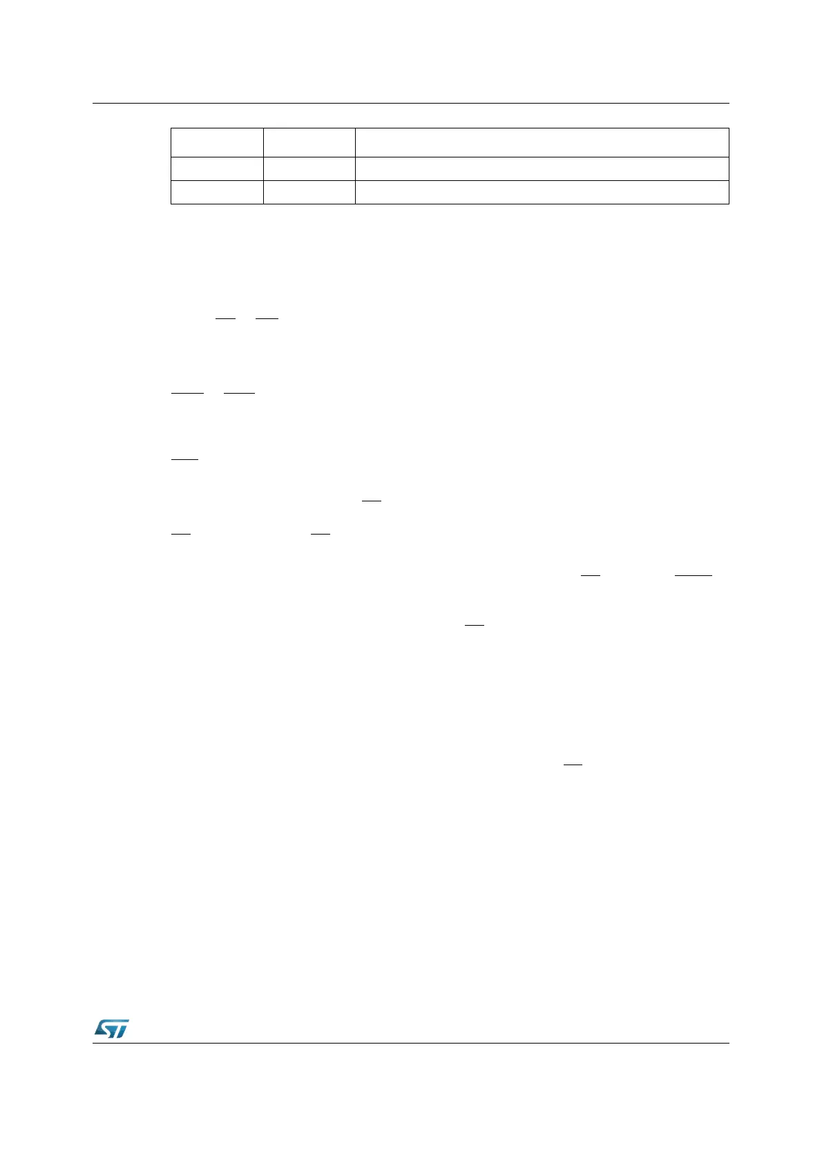
1 0 Write Chip Select
1 1 Read/Write Chip Select
CSWENx CSRENx Chip select mode