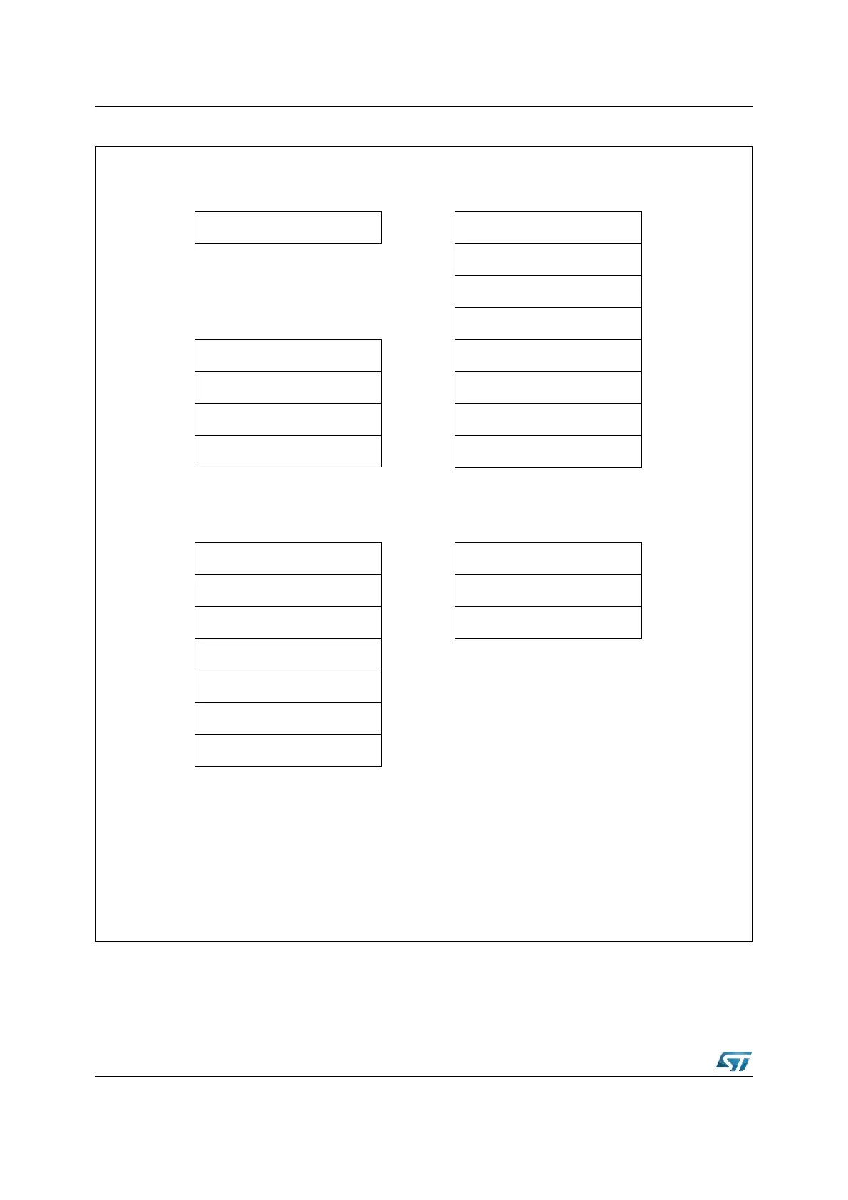
Figure 151. XBUS registers and port pins associated with the XPWM module
Ports & Direction Control Alternate Functions Data Registers
15
-
14
-
13
-
12
-
11
Y
10
Y
9
Y
8
Y
7
Y
6
Y
5
Y
4
Y
3
Y
2
Y
1
Y
0
YXPWMPORT XPP0
15
Y
14
Y
13
Y
12
Y
11
Y
10
Y
9
Y
8
Y
7
Y
6
Y
5
Y
4
Y
3
Y
2
Y
1
Y
0
Y
XPW0 YYYY
Y Y YYYYYYYYYY
XPP1 Y Y Y Y
Y Y YYYYYYYYYY
Counter Registers
Interrupt Control
15
Y
14
Y
13
Y
12
Y
11
Y
10
Y
9
Y
8
Y
7
Y
6
Y
5
Y
4
Y
3
Y
2
Y
1
Y
0
YXPT0
15 14 13 12 11 10 9 8 7 6 5 4 3 2 1 0
XPWMCON0 YYYY
Y Y YYYYYYYYYY
XPW1 YYYYY Y YYYYYYYYYY
XPP2 Y Y Y Y Y Y YYYYYYYYYY
XPW2 YYYYY Y YYYYYYYYYY
XPP3 Y Y Y Y
Y Y YYYYYYYYYY
XPW3 YYYYY Y YYYYYYYYYY
YYYY
Y Y YYYYYYYYYYXPT1
XPWMPORT XPWM Port Control Register
XPPx XPWM Period Register x
XPWx XPWM Pulse Width Register x
XPTx XPWM Counter Register x
XPOLAR XPWM Channel Polarity Register
XPOUT0 / P8.0
XPOUT1 / P8.1
XPOUT2 / P8.2
XPOUT3 / P8.3
XIRxSEL XPxINT Interrupt Selection Control Register
XIRxSET XPxINT Interrupt Selection Control Reg. Bit Set
XIRxCLR XPxINT Interrupt Selection Control Reg. Bit Clear
XPWMCONx XPWM Control Register 0/1
XPWMCONxSETXPWM Control Register 0/1 Bit Set (write only)
XPWMCONxCLRXPWM Control Register 0/1 Bit Clear (write only)
YYYYY Y YYYYYYYYYYXPT2
YYYYY Y YYYYYYYYYYXPT3
XPWMCON0SETYYYY
Y Y YYYYYYYYYY
XIRxSEL Y Y Y Y Y Y YYYYYYYYYY
XIRxSET Y Y Y Y Y Y YYYYYYYYYY
XIRxCLR Y Y Y Y Y Y YYYYYYYYYY
15 14 13 12 11 10 9 8 7 6 5 4 3 2 1 0
Control Registers
XPWMCON0CLRYYYYY Y YYYYYYYYYY
XPWMCON1 Y Y - Y
- - - - YYYYYYYY
XPWMCON1SET Y Y - Y - - - - YYYYYYYY
XPWMCON1CLR Y Y - Y - - - - YYYYYYYY
----- - ------YYYYXPOLAR
Bit is linked to a function
Bit has no function or is not implemented
Y
-
:
: