The central processing unit (CPU) UM0404
72/564 DocID13284 Rev 2
The CSP register can only be read but not written by data operations. It is, however,
modified either directly by means of the JMPS and CALLS instructions, or indirectly via the
stack by means of the RETS and RETI instructions.
Upon the acceptance of an interrupt or the execution of a software TRAP instruction, the
CSP register is automatically set to zero.
3.4.8 The data page pointers DPP0, DPP1, DPP2, DPP3
These four non-bit-addressable registers select up to four different data pages being active
simultaneously at run-time. The lower 10 bits of each DPP register select one of the 1024
possible 16 Kbyte data pages while the upper 6 bits are reserved for future use. The DPP
registers make it possible to access the entire memory space, in pages of 16 Kbytes each.
The DPP registers are implicitly used whenever data accesses to any memory location are
made via indirect, or direct long 16-bit addressing modes (except for override accesses via
EXTended instructions and PEC data transfers). After reset, the Data Page Pointers are
initialized in a way that all indirect or direct long 16-bit addresses result in identical 18-bit
addresses. This allows to access data pages 3...0 within segment 0 as shown in the
Figure 13 on page 73. If the user does not want to use any data paging, no further action is
required.
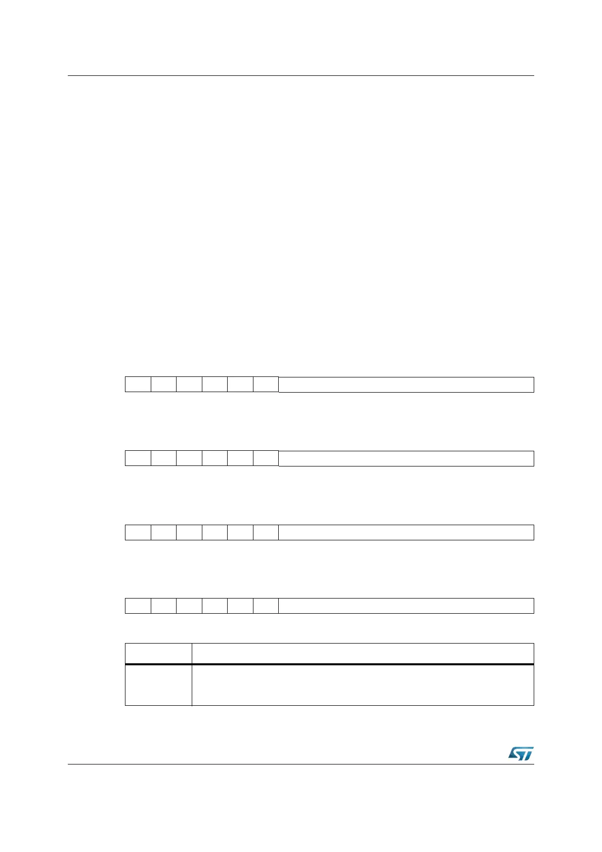
DPP0 (FE00h / 00h) SFR Reset Value: 0000h
DPP1 (FE02h / 01h) SFR Reset Value: 0001h
DPP2 (FE04h / 02h) SFR Reset Value: 0002h
DPP3 (FE06h / 03h) SFR Reset Value: 0003h
1514131211109876543210
------ DPP0PN
RW
1514131211109876543210
------ DPP1PN
RW
1514131211109876543210
------ DPP2PN
RW
1514131211109876543210
------ DPP3PN
RW
Bit Function
DPPxPN
Data Page Number of DPPx
Specifies the data page selected via DPPx. Only the 2 least significant bits of DPPx
are used when segmentation is disabled.