Parallel ports UM0404
160/564 DocID13284 Rev 2
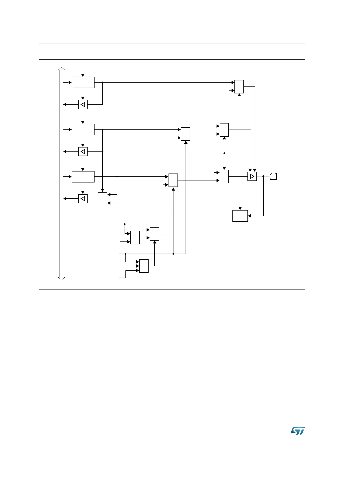
Figure 42. Block diagram of P4.6 pin
Note: When SALSEL = ‘10’, that is 8-bit segment address lines are selected, P4.6 is dedicated to
output the address: any attempt to use the CAN1 on P4.6 is masked.
When CAN parallel mode is selected, CAN2_TxD is remapped on P4.6: this occurs only if
CAN1 is enabled as well. On the contrary, if CAN1 is disabled, no remapping occurs.
MUX
0
1
P4.6
Open Drain
Latch
Write ODP4.6
Read ODP4.6
Direction
Latch
Write DP4.6
Read DP4.6
Port Output
Latch
Write P4.6
Read P4.6
MUX
1
0
MUX
1
0
‘0’
CAN2_TxD
Data Output
Output
Buffer
Input
Latch
Clock
XMISC.1
(CANPAR)
I
n
t
e
r
n
a
l
B
u
s
&
MUX
1
0
CAN1_TxD
Data Output
XPERCON.0
(CAN1EN)
MUX
1
0
Ext. Memory
Data Output
MUX
1
0
‘1’
Ext. Memory
Function
MUX
0
1
Enable
‘1’
XPERCON.1
(CAN2EN)
&