Parallel ports UM0404
158/564 DocID13284 Rev 2
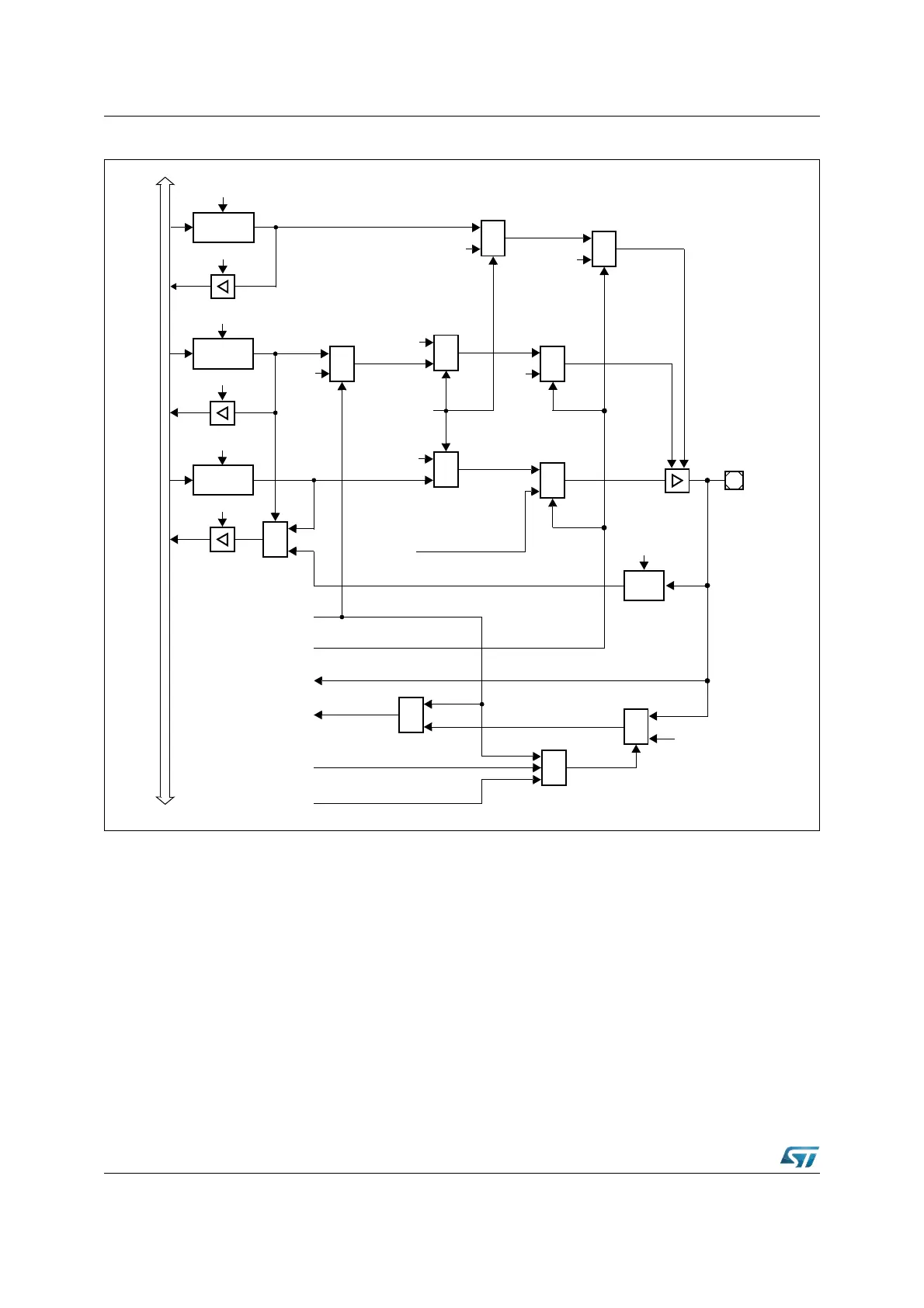
Figure 40. Block diagram of P4.4 pin
Note: When SALSEL = ‘10’, that is 8-bit segment address lines are selected, P4.4 is dedicated to
output the address: any attempt to use the CAN2 on P4.4 is masked. On the contrary,
enabling the I
2
C, also the segment function is masked; the pin P4.4 is automatically
configured as open-drain and used to input and output SCL alternate function.
When CAN parallel mode is selected, CAN2_RxD is remapped on P4.5: this occurs only if
CAN1 is enabled as well. On the contrary, if CAN1 is disabled, no remapping occurs.
P4.4
Direction
Latch
Write DP4.4
Read DP4.4
Port Output
Latch
Write P4.4
Read P4.4
MUX
1
0
MUX
1
0
Ext. Memory
Data Output
MUX
1
0
‘1’
Ext. Memory
Function
Output
Buffer
MUX
0
1
Input
Latch
Clock
XPERCON.1
(CAN2EN)
SCL
Data Input
I
n
t
e
r
n
a
l
B
u
s
Enable
SCL
Data Output
XPERCON.9
(I2CEN)
MUX
1
0
MUX
0
1
CAN2_RxD
Data Input
XMISC.1
(CANPAR)
P4.5
‘0’
&
&
XPERCON.0
(CAN1EN)
MUX
1
0
‘1’
MUX
0
1
Open Drain
Latch
Write ODP4.4
Read ODP4.4
‘0’
MUX
0
1
‘1’