Asynchronous / synchronous serial interface UM0404
252/564 DocID13284 Rev 2
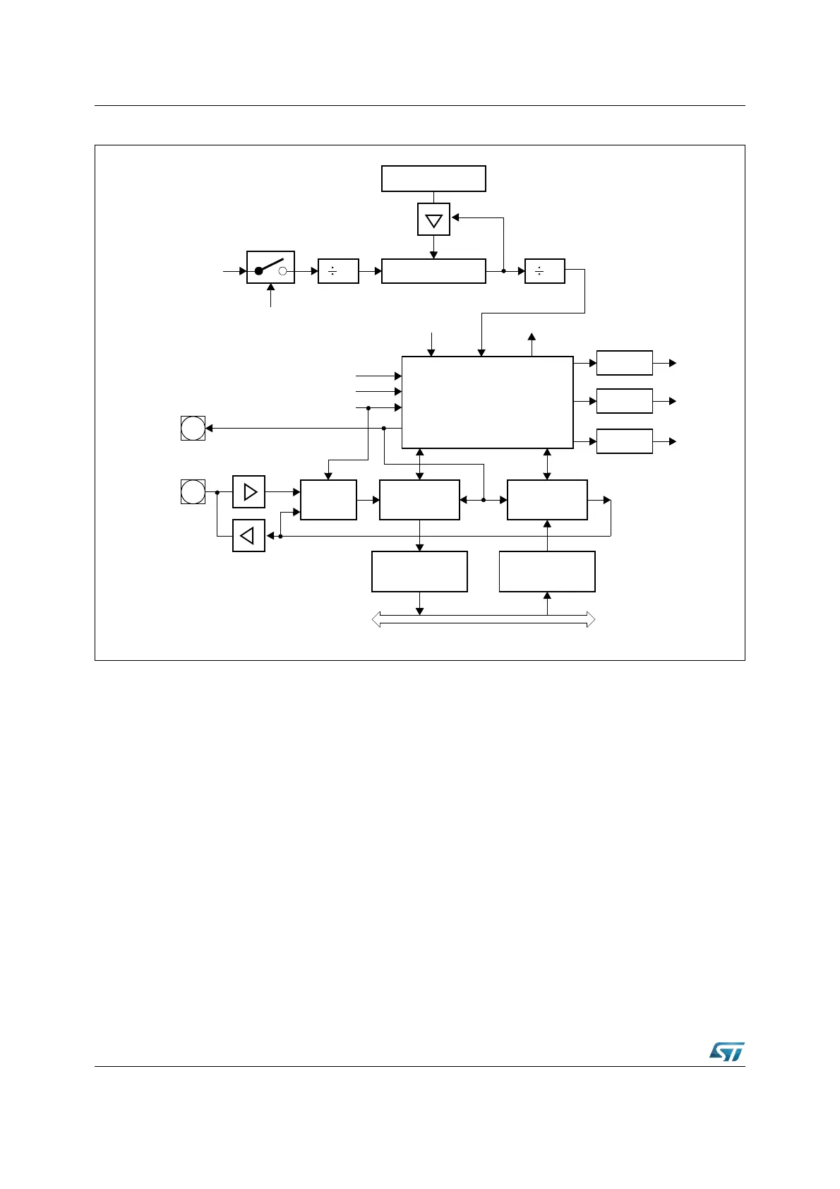
Figure 103. Synchronous mode of serial channel ASC0
Synchronous transmission begins within four CPU clock cycles after data has been
loaded into S0TBUF, provided that S0R is set and S0REN = ‘0’ (half-duplex, no reception).
Data transmission is double buffered. When the transmitter is idle, the transmit data loaded
into S0TBUF is immediately moved to the transmit shift register thus freeing S0TBUF for the
next data to be sent. This is indicated by the transmit buffer interrupt request flag S0TBIR
being set. S0TBUF may now be loaded with the next data, while transmission of the
previous one is still going on. The data bits are transmitted synchronous with the shift clock.
After the bit time for the 8th data bit, both pins TXD0 and RXD0 will go high, the transmit
interrupt request flag S0TIR is set, and serial data transmission stops.
Pin TXD0/P3.10 must be configured for alternate data output, P3.10 = ‘1’ and DP3.10 = ‘1’,
in order to provide the shift clock. Pin RXD0/P3.11 must also be configured for output
(P3.11 = ‘1’ and DP3.11 = ‘1’) during transmission.
Synchronous reception is initiated by setting bit S0REN = ‘1’. If bit S0R = ‘1’, the data
applied at pin RXD0 are clocked into the receive shift register synchronous to the clock
which is output at pin TXD0. After the 8th bit has been shifted in, the content of the receive
shift register is transferred to the receive data buffer S0RBUF, the receive interrupt request
flag S0RIR is set, the receiver enable bit S0REN is reset, and serial data reception stops.
2
CPU
Clock
S0R
Baud Rate Timer
Reload Register
4
Clock
Serial Port Control
Shift Clock
S0M = 000b S0OE
S0REN
S0OEN
S0LB
S0RIR
S0TIR
S0EIR
Receive
Interrupt
Transmit
Interrupt
Error
Interrupt
Transmit Shift
Register
Receive Shift
Register
Transmit Buffer
Register S0TBUF
Receive Buffer
Register S0RBUF
MUX
0
1
Internal Bus
Receive
Output
Transmit
RXD0
TDX0
P3.11
Input / Output
P3.10
Request
Request
Request
 Loading...