DocID13284 Rev 2 387/564
UM0404 Analog / digital converter
assuming a conversion rate of 250 kHz, with C
S
equal to 4pF, a resistance of 1MΩ is
obtained (R
EQ
= 1 / f
C
C
S
, where f
C
represents the conversion rate at the considered
channel). To minimize the error induced by the voltage partitioning between this resistance
(sampled voltage on C
S
) and the sum of R
S
+ R
F
+ R
L
+ R
SW
+ R
AD
, the external circuit
must be designed to respect the following relation:
The formula above provides a constraints for external network design, in particular on
resistive path.
A second aspect involving the capacitance network should be considered. Assuming the
three capacitances C
F
, C
P1
and C
P2
initially charged at the source voltage V
A
(refer to the
equivalent circuit reported in Figure 165), when the sampling phase is started (A/D switch
close), a charge sharing phenomena is installed.
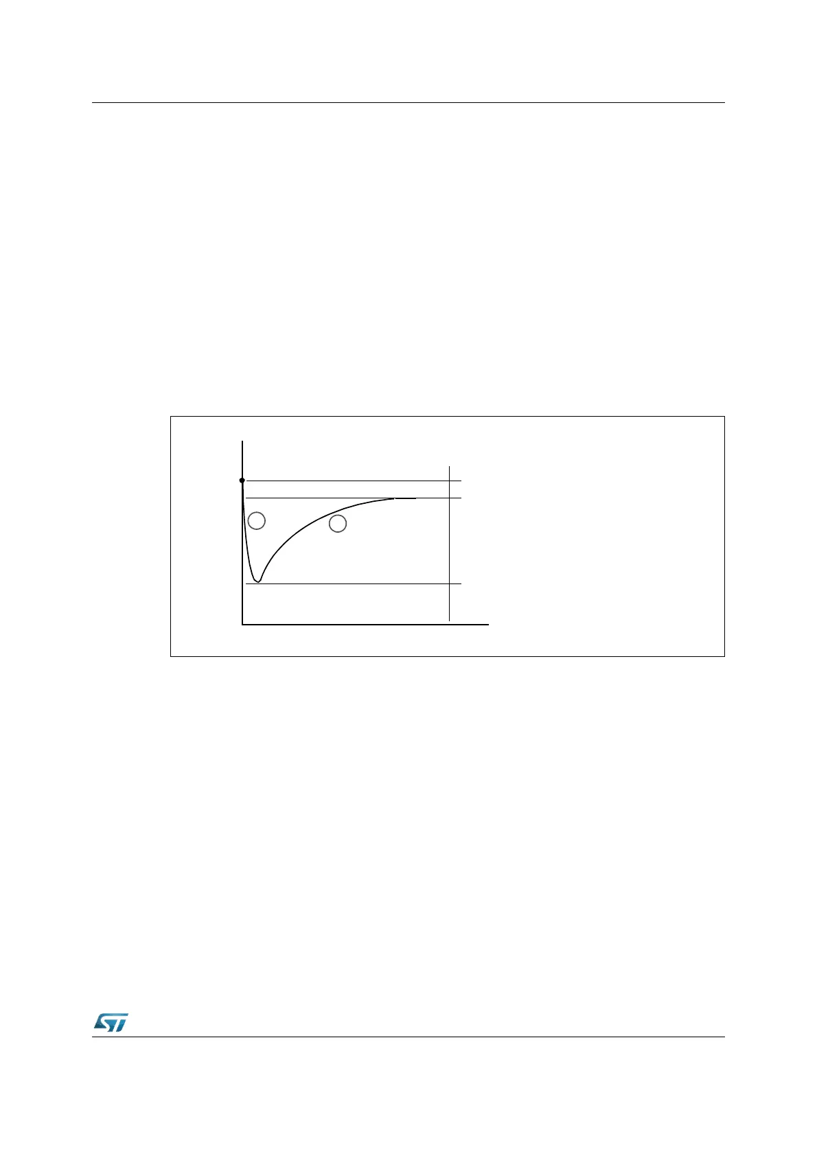
Figure 166. Charge sharing timing diagram during sampling phase
In particular two different transient periods can be distinguished (see Figure 166):
• A first and quick charge transfer from the internal capacitance C
P1
and C
P2
to the
sampling capacitance C
S
occurs (C
S
is supposed initially completely discharged):
considering a worst case (since the time constant in reality would be faster) in which
C
P2
is reported in parallel to C
P1
(call C
P
= C
P1
+ C
P2
), the two capacitance C
P
and C
S
are in series, and the time constant is:
• This relation can again be simplified considering only C
S
as an additional worst
condition. In reality, the transient is faster, but the A/D Converter circuitry has been
V
A
R
S
R
F
R
L
R
SW
R
AD
+++ +
R
EQ
-------------------------------------------------------------
⋅
1
2
---
LSB
<
V
A
V
A1
V
A2
t
T
S
V
CS
Voltage Transient on C
S
ΔV < 0.5 LSB
1
2
τ
1
< (R
SW
+ R
AD
) C
S
<< T
S
τ
2
= R
L
(C
S
+ C
P1
+ C
P2
)
τ
1
R
SW
R
AD
+()=
C
P
C
S
⋅
C
P
C
S
+
-----------------------
⋅