Parallel ports UM0404
154/564 DocID13284 Rev 2
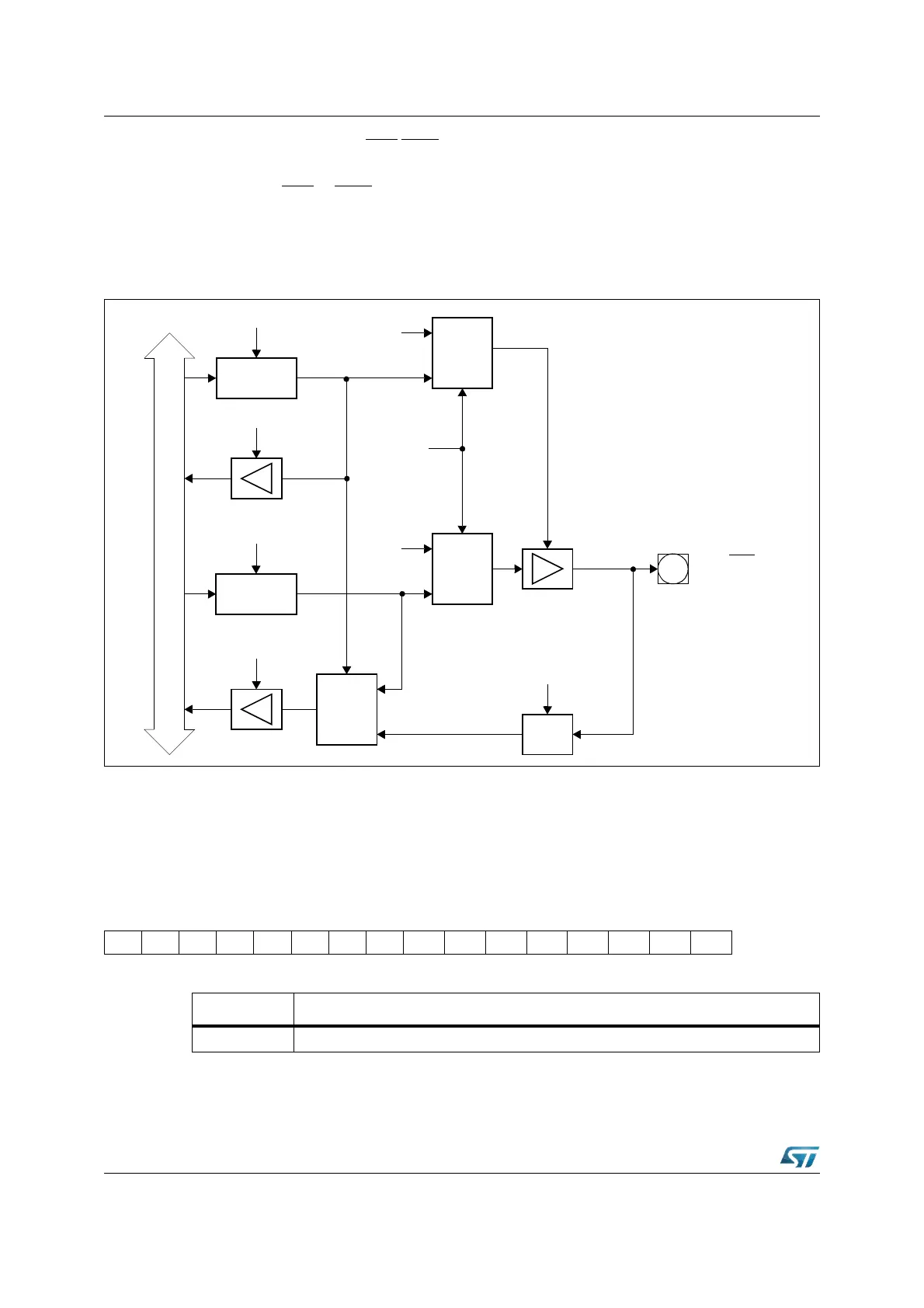
selected automatically. If BHE/WRH is not used in the system, this pin can be used for
general purpose I/O by disabling the alternate function (BYTDIS = ‘1’ / WRCFG = ‘0’).
Note: Enabling the BHE
or WRH function automatically enables the P3.12 output driver. Setting bit
DP3.12 = ‘1’ is not required.
During bus hold pin P3.12 is switched back to its standard function and is then controlled by
DP3.12 and P3.12. Keep DP3.12 = ’0’ in this case to ensure floating in hold mode.
Figure 37. Block diagram of P3.15 (CLKOUT) and P3.12 (BHE/WRH) pins
6.6 Port4
If this 8-bit port is used for general purpose I/O, the direction of each line can be configured
via the corresponding direction register DP4.
P4 (FFC8h / E4h) SFR Reset Value: - - 00h
Direction
Latch
Write DP3.x
Read DP3.x
Port Output
Latch
Write P3.x
Read P3.x
Internal Bus
MUX
0
1
MUX
0
1
Alternate
Data
Output
MUX
0
1
“1”
Input
Latch
Clock
P3.12/BHE
P3.15/CLKOUT
Output
Buffer
x = 15, 12
Alternate
Function
Enable
1514131211109876543210
- - - - - - - - P4.7 P4.6 P4.5 P4.4 P4.3 P4.2 P4.1 P4.0
RW RW RW RW RW RW RW RW
Bit Function
P4.y Port data register P4 bit y