DocID13284 Rev 2 349/564
UM0404 Pulse width modulation module
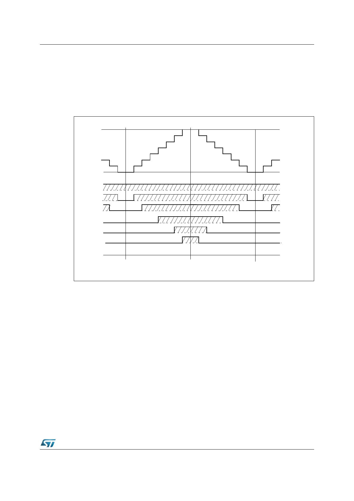
Note that in mode 1 the period of the PWM signal is twice the period of the timer:
PWM_Period
Mode1
= 2 x ([PPx] + 1)
Figure 147 illustrates the operation and output waveforms of a PWM channel in mode 1 for
different values in the pulse width register. This mode is referred to as Center Aligned PWM,
because the value in the pulse width shadow register effects both edges of the output signal
symmetrically.
Figure 147. Operation and output waveform in mode 1
17.1.3 Burst mode
Burst mode is selected by setting bit PB01 in register PWMCON1 to ‘1’. This mode
combines the signals from PWM channels 0 and 1 onto the port pin of channel 0.
The output of channel 0 is replaced with the logical AND of channels 0 and 1. The output of
channel 1 can still be used at its associated output pin (if enabled).
Each of the two channels can either operate in mode 0 or 1.
Note: It is guaranteed by design, that no spurious spikes will occur at the output pin of channel 0 in
this mode. The output of the AND gate will be transferred to the output pin synchronously to
internal clocks.XORing of the PWM signal and the port output latch value is done after the
ANDing of channel 0 and 1 (see Figure 148).
1
7
6
5
3
4
2
1
0
1
0
PPx
Period=7
PTx Count
Value
PWx Pulse
Width=0
PWx=1
PWx=2
PWx=4
PWx=6
PWx=7
PWx=8
Latch Shadow Registers
Interrupt Reques
Change Count
LSR
Duty Cycle
100%
87.5%
75%
50%
25%
12.5%
0%
0
2
7
6
5
4
3
2
1
Direction
LSR