DocID13284 Rev 2 383/564
UM0404 Analog / digital converter
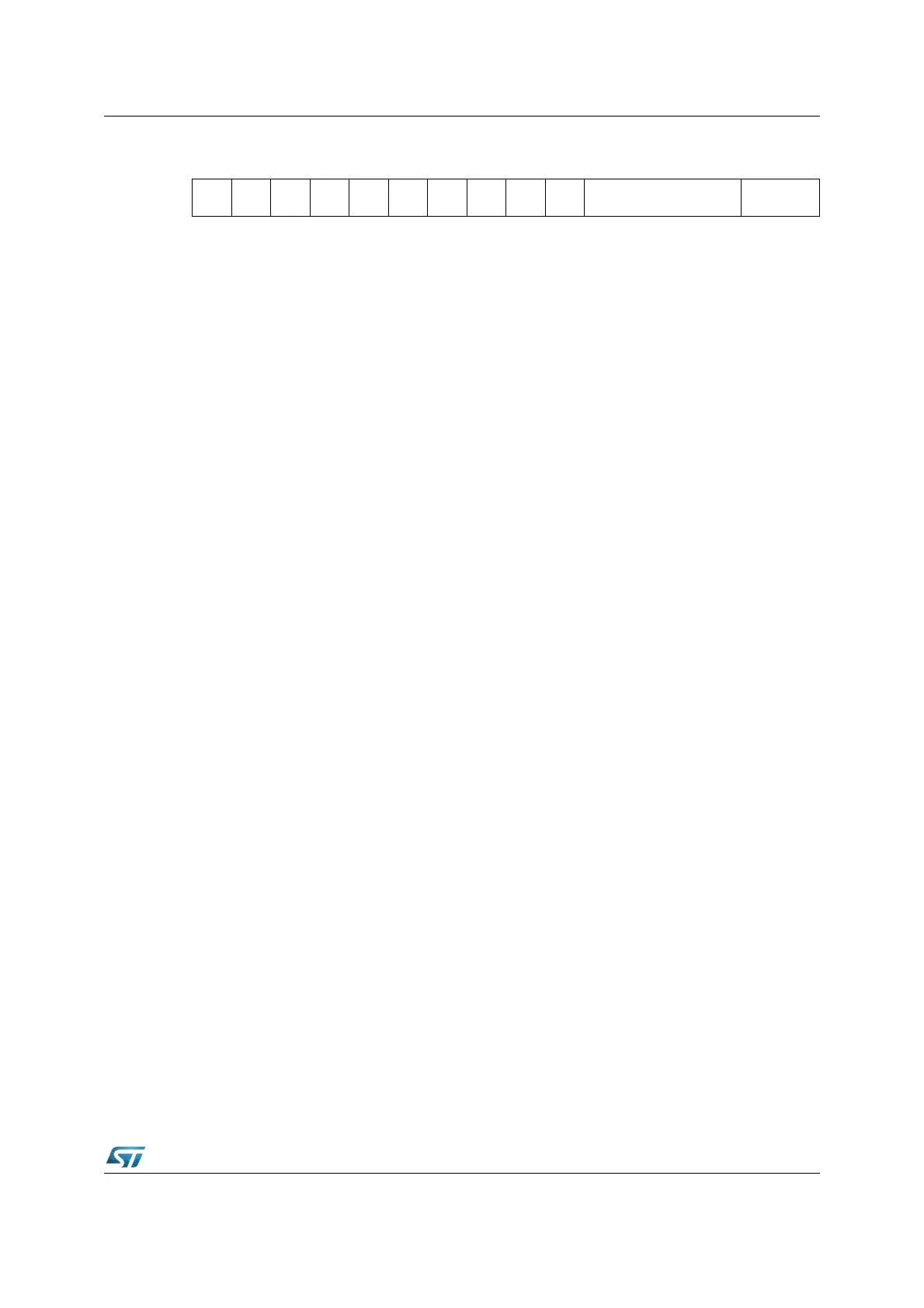
ADEIC (FF9Ah / CDh) SFR Reset Value: - - 00h
Note: Refer to Section 5.1.3: Interrupt control registers on page 100 for explanation of the control
fields.
19.4 Calibration
A full calibration sequence is performed after a reset. This full calibration lasts 40.629 ± 1
CPU clock cycles. During this time, the busy flag ADBSY is set to indicate the operation. It
compensates the capacitance mismatch, so the calibration procedure does not need any
update during normal operation.
No conversion can be performed during this time: the bit ADBSY should be polled to verify
when the calibration is over, and the module is able to start a conversion.
Since the calibration process writes repeatedly spurious conversion results inside ADDAT
register, at the end of the calibration, both ADCIR and ADEIR flags are set. For this reason,
before starting a conversion, in the A/D Converter initialization routine, the application
should perform a dummy read of ADDAT register and clear the two flags.
Note: If ADDAT is not read before starting the first conversion, and for example “Wait for Read
Mode” is entered (ADWR bit set), the A/D Converter is stack waiting for the ADDAT read,
since the result of the current conversion cannot be immediately written inside ADDAT,
which contains the results of the calibration (meaningless data).
19.5 A/D conversion accuracy
The A/D Converter compares the analog voltage sampled on the selected analog input
channel to its analog reference voltage (V
AREF
) and converts it into 10-bit digital data. The
absolute accuracy of the A/D conversion is the deviation between the input analog value
and the output digital value. It includes the following errors:
• Offset error (OFS)
• Gain Error (GE)
• Quantization error
• Non-Linearity error (Differential and Integral)
These four error quantities are explained below using Figure 164.
Offset Error
Offset error is the deviation between actual and ideal A/D conversion characteristics when
the digital output value changes from the minimum (zero voltage) 00 to 01 (Figure 164, see
OFS).
Gain Error
Gain error is the deviation between the actual and ideal A/D conversion characteristics
when the digital output value changes from the 3FE to the maximum 3FF, once offset error
is subtracted.
1514131211109876543210
--------
ADE
IR
ADE
IE
ILVL GLVL
RW RW RW RW