The external bus interface UM0404
194/564 DocID13284 Rev 2
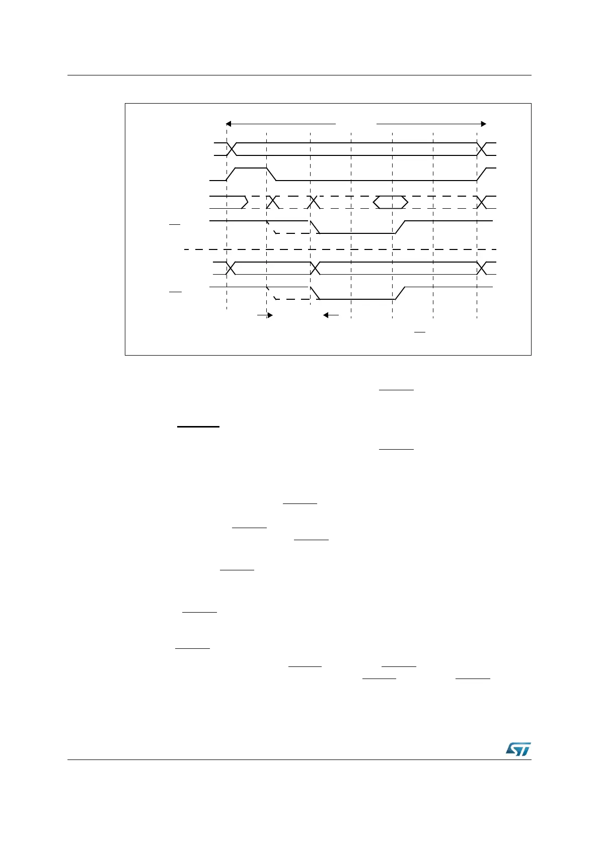
Figure 65. Read / write delay
8.3.5 READY polarity
The active level of the ready pin can be set to READY or READY by the RDYPOL bit 13 in
the BUSCON register.
8.3.6 READY / READY controlled bus cycles
The active level of the ready pin can be set to READY or READY by the RDYPOL bit in the
BUSCON register.
For situations where the programmable wait-states are not enough, or where the response
(access) time of a peripheral is not constant, the ST10F276 provides external bus cycles
that are terminated by a READY or READY
input signal (synchronous or asynchronous). In
this case the ST10F276 first inserts a programmable number of wait-states (0...7) and then
monitors the READY or READY
line to determine the actual end of the current bus cycle.
The external device drives READY or READY
low in order to indicate that data have been
latched (write cycle) or are available (read cycle).
When the READY or READY
function is enabled for a specific address window, each bus
cycle in this window must be terminated with the active level defined by the RDYPOL bit in
the associated BUSCON register (see Figure 66).
The READY/READY
function is enabled by the RDYENx bit in the BUSCON registers.
When this function is selected (RDYENx = ‘1’), only the lower 3 bits of the respective MCTC
bit-field define the number of inserted wait-states (0...7), while the MSB of bit-field MCTC
selects the READY
operation:
MCTC.3 = ‘0’: Synchronous READY/READY
, the READY/READY signal must meet setup
and hold times. MCTC.3 = ‘1’: Asynchronous READY/READY
, the READY/READY signal is
synchronized internally.
1) The data drivers from the previous bus cycle should be disabled when the RD signal becomes active.
Read / Write
Bus Cycle
Segment
ALE
BUS (P0)
RD
BUS (P0)
WR
Address
Address
Data/Instr.
Data
1)
Delay