Parallel ports UM0404
142/564 DocID13284 Rev 2
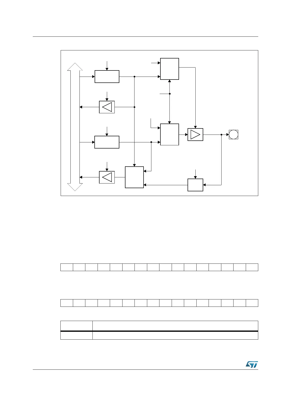
Figure 29. Block diagram of a PORT0 pin
6.3 PORT1
The two 8-bit ports P1H and P1L represent the higher and lower part of PORT1,
respectively. Both halves of PORT1 can be written (for example via a PEC transfer) without
effecting the other half. If this port is used for general purpose I/O, the direction of each line
can be configured via the corresponding direction registers DP1H and DP1L.
P1L (FF04h / 82h) SFR Reset Value: - - 00h
P1H (FF06h / 83h) SFR Reset Value: - - 00h
Direction
Latch
Write DP0H.y / DP0L.y
Read DP0H.y / DP0L.y
Port Output
Latch
Write P0H.y / P0L.y
Read P0H.y / P0L.y
Internal Bus
MUX
0
1
MUX
0
1
Alternate
Data
Output
MUX
0
1
Alternate
Direction
Input
Latch
Clock
P0H.y
P0L.y
Output
Buffer
y = 7...0
Alternate
Function
Enable
Port Data
Output
1514131211109876543210
- - - - - - - - P1L.7 P1L.6 P1L.5 P1L.4 P1L.3 P1L.2 P1L.1 P1L.0
RW RW RW RW RW RW RW RW
1514131211109876543210
- - - - - - - - P1H.7P1H.6P1H.5P1H.4P1H.3P1H.2P1H.1P1H.0
RW RW RW RW RW RW RW RW
Bit Function
P1X.y Port data register P1H or P1L bit y