Parallel ports UM0404
152/564 DocID13284 Rev 2
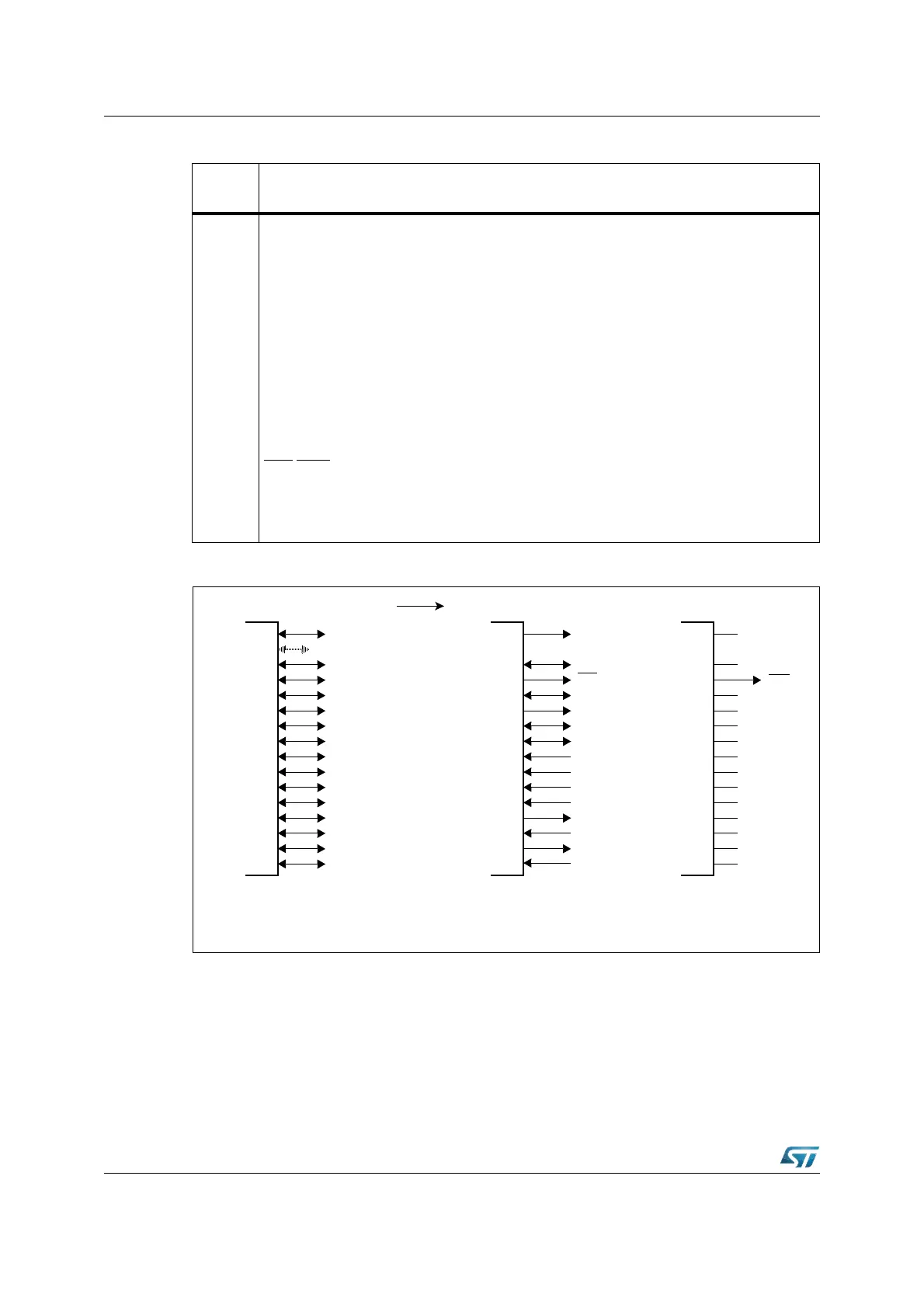
Figure 35. Port3 I/O and alternate functions
The structure of the Port3 pins depends on their alternate function (see Figure 36).
When the on-chip peripheral associated with a Port3 pin is configured to use the alternate
input function, it reads the input latch, which represents the state of the pin, via the line
labeled “Alternate Data Input”. Port3 pins with alternate input functions are: T0IN, T2IN,
T3IN, T4IN, T3EUD and CAPIN.
When the on-chip peripheral associated with a Port3 pin is configured to use the alternate
output function, its “Alternate Data Output” line is ANDed with the port output latch line.
Table 23. Port3 alternative functions
Port3
pin
Alternate function
P3.0
P3.1
P3.2
P3.3
P3.4
P3.5
P3.6
P3.7
P3.8
P3.9
P3.10
P3.11
P3.12
P3.13
P3.14
P3.15
T0IN CAPCOM1 Timer 0 Count Input
T6OUT Timer 6 Toggle Output
CAPIN GPT2 Capture Input
T3OUT Timer 3 Toggle Output
T3EUD Timer 3 External Up/Down Input
T4IN Timer 4 Count Input
T3IN Timer 3 Count Input
T2IN Timer 2 Count Input
MRST0 SSC Master Receive / Slave Transmit
MTSR0 SSC Master Transmit / Slave Receive
TxD0 ASC0 Transmit Data Output
RxD0 ASC0 Receive Data Input (/ Output in synchronous mode)
BHE
/WRH Byte High Enable / Write High Output
SCLK0 SSC Shift Clock Input/Output
--- No pin assigned
CLKOUT System Clock Output (either prescaled or not through register XCLKOUTDIV)
Port3
No Pin
Alternate Functions a) b)
General Purpose
Input/Output
P3.7
P3.6
P3.5
P3.4
P3.3
P3.2
P3.1
P3.0
P3.15
P3.13
P3.12
P3.11
P3.10
P3.9
P3.8
T2IN
T3IN
T4IN
T3EUD
T3OUT
CAPIN
T6OUT
T0IN
CLKOUT
SCLK0
BHE
RxD0
TxD0
MTSR0
MRST0
WRH