Memory organization UM0404
42/564 DocID13284 Rev 2
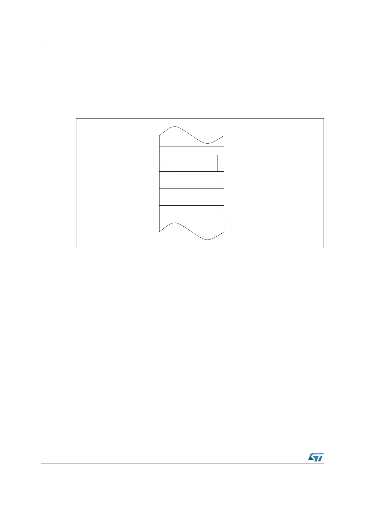
Double words (code only) are stored in ascending memory locations as two subsequent
words. Single bit are always stored in the specified bit position at a word address.
Bit position 0 is the least significant bit of the byte at an even byte address, and bit position
15 is the most significant bit of the byte at the next odd byte address. Bit addressing is
supported for a part of the Special Function Registers, a part of the IRAM and for the
General Purpose Registers.
Figure 5. Storage of words, bytes and bits in a byte organized memory
Note: Byte units forming a single word or a double word must always be stored within the same
physical (internal, external, Flash, RAM) and organizational (page, segment) memory area.
2.2 On-chip Flash
The ST10F276 reserves an address area of 512+320 Kbytes for on-chip Flash memory.
In standard mode (the normal operating mode) the first portion (512 Kbytes) of the Flash
(IFlash) appears like an on-chip ROM with the same timing and functionality. The IFlash
module offers a fast access time, allowing zero wait-state access with CPU frequency up to
64 MHz. Instruction fetches and data operand reads are performed with all addressing
modes of the ST10F276 instruction set. The second portion (320 Kbytes) appears like an
on-chip X-Peripheral: it can be accessed like an external memory in 16-bit demultiplexed
bus-mode without read/write delay at zero wait-states with CPU frequency up to 40 MHz,
while one wait-state should be added for higher frequency rates.
In order to optimize the programming time of the internal Flash, up to four different Banks
divided in blocks of 8 Kbytes, 16 Kbytes, 32 Kbytes and 64 Kbytes can be used. Reading
from one Bank while programming another Bank is possible. For a complete memory
mapping summary, see details in Table 3 and Table 4.
In the table below, the Segment 8 address range mapping is summarized, varying ROMEN
(related with EA
pin status under reset) and XPEN bits status in SYSCON register and
XPERCON (bits XRAM2EN and XFLASHEN) programming.
...
... Bit ...
... Bit ...
Byte
Byte
Word (high byte)
Word (low byte)
15 14 8
76 0
xxxx6h
xxxx5h
xxxx4h
xxxx3h
xxxx2h
xxxx1h
xxxx0h
xxxxFh
...