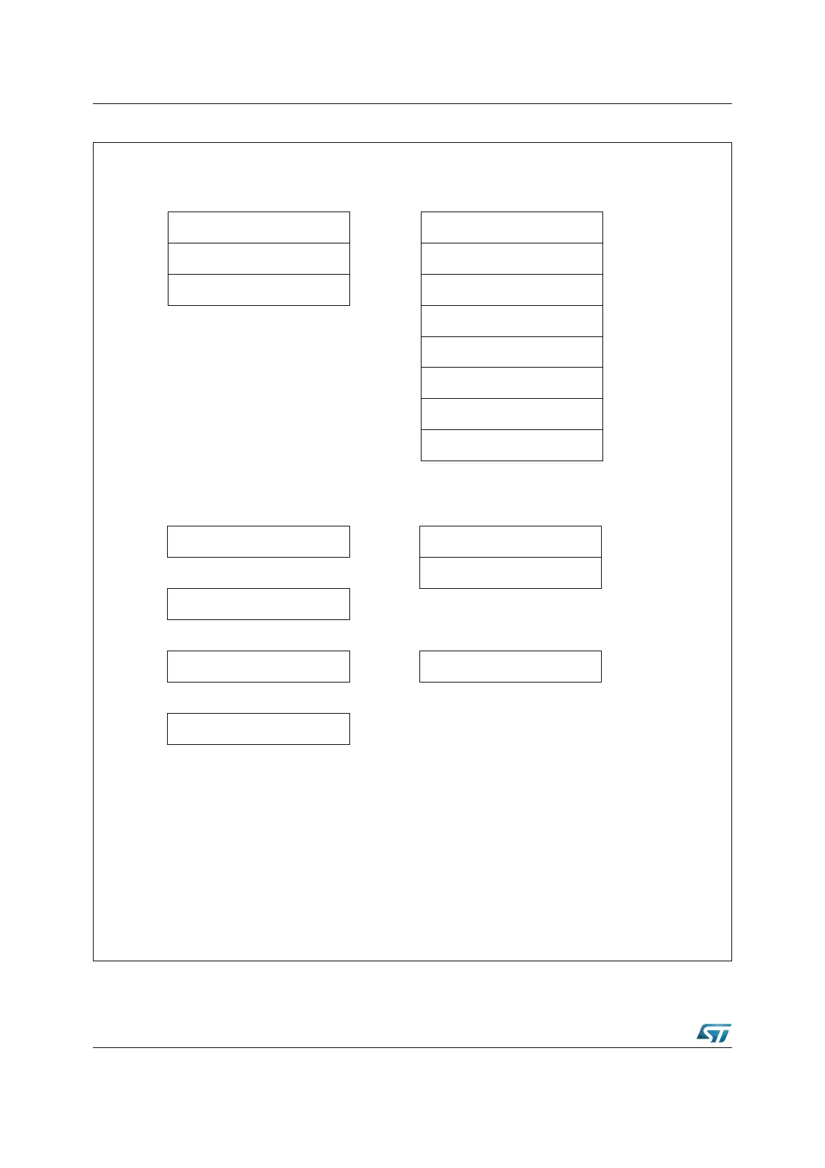
Figure 144. SFRs and port pins associated with the PWM module
Ports & Direction Control Alternate Functions Data Registers
15
-
14
-
13
-
12
-
11
-
10
-
9
-
8
-
7
-
6
-
5
-
4
-
3
Y
2
Y
1
Y
0
YODP7 E PP0 E
15
Y
14
Y
13
Y
12
Y
11
Y
10
Y
9
Y
8
Y
7
Y
6
Y
5
Y
4
Y
3
Y
2
Y
1
Y
0
Y
----
- - ------YYYYDP7
----
- - ------YYYYP7
PW0 YYYY
Y Y YYYYYYYYYY
PP1 E YYYY
Y Y YYYYYYYYYY
Control Registers Interrupt Control
15
Y
14
Y
13
Y
12
Y
11
Y
10
Y
9
Y
8
Y
7
Y
6
Y
5
Y
4
Y
3
Y
2
Y
1
Y
0
YPT0 E
15 14 13 12 11 10 9 8 7 6 5 4 3 2 1 0
PWMCON0
----
- - - - YYYYYYYYPWMIC E
YYYY
Y Y YYYYYYYYYY
PW1 YYYY
Y Y YYYYYYYYYY
PP2 E YYYYY Y YYYYYYYYYY
PW2 YYYY
Y Y YYYYYYYYYY
PP3 E YYYY
Y Y YYYYYYYYYY
PW3 YYYYY Y YYYYYYYYYY
YYYY
Y Y YYYYYYYYYYPT1 E
ODP7 Port7 Open Drain Control Register
DP7 Port7 Direction Control Register
P7 Port7 Data Register
PWMICPWM Interrupt Control Register
POUT0/P7.0
POUT1/P7.1
POUT2/P7.2
POUT3/P7.3
PPx PWM Period Register x
PWx PWM Pulse Width Register x
PTx PWM Counter Register x
PWMCONxPWM Control Register 0/1
YYYYY Y YYYYYYYYYYPT2 E
YYYY
Y Y YYYYYYYYYYPT3 E
PWMCON1 YYYY
Y Y YYYYYYYYYY
Bit is linked to a function
Bit has no function or is not implemented
Register is in ESFR internal memory space
Y
-
E
:
:
: