DocID13284 Rev 2 197/564
UM0404 The external bus interface
The properties of a bus cycle like chip select mode, usage of READY, length of ALE,
external bus mode, read/write delay and wait-states are controlled by
BUSCON4...BUSCON0 registers. Four of these registers (BUSCON4...BUSCON1) have an
associated address select register (ADDRSEL4...ADDRSEL1) which allows to specify up to
four address areas and the individual bus characteristics within these areas. All accesses
that are not covered by these four areas are then controlled via BUSCON0. This allows to
use memory components or peripherals with different interfaces within the same system,
while optimizing accesses to each of them.
BUSCON4...BUSCON0 bit SGTDIS controls the correct stack operation (push/pop of CSP
or not) during traps and interrupts.
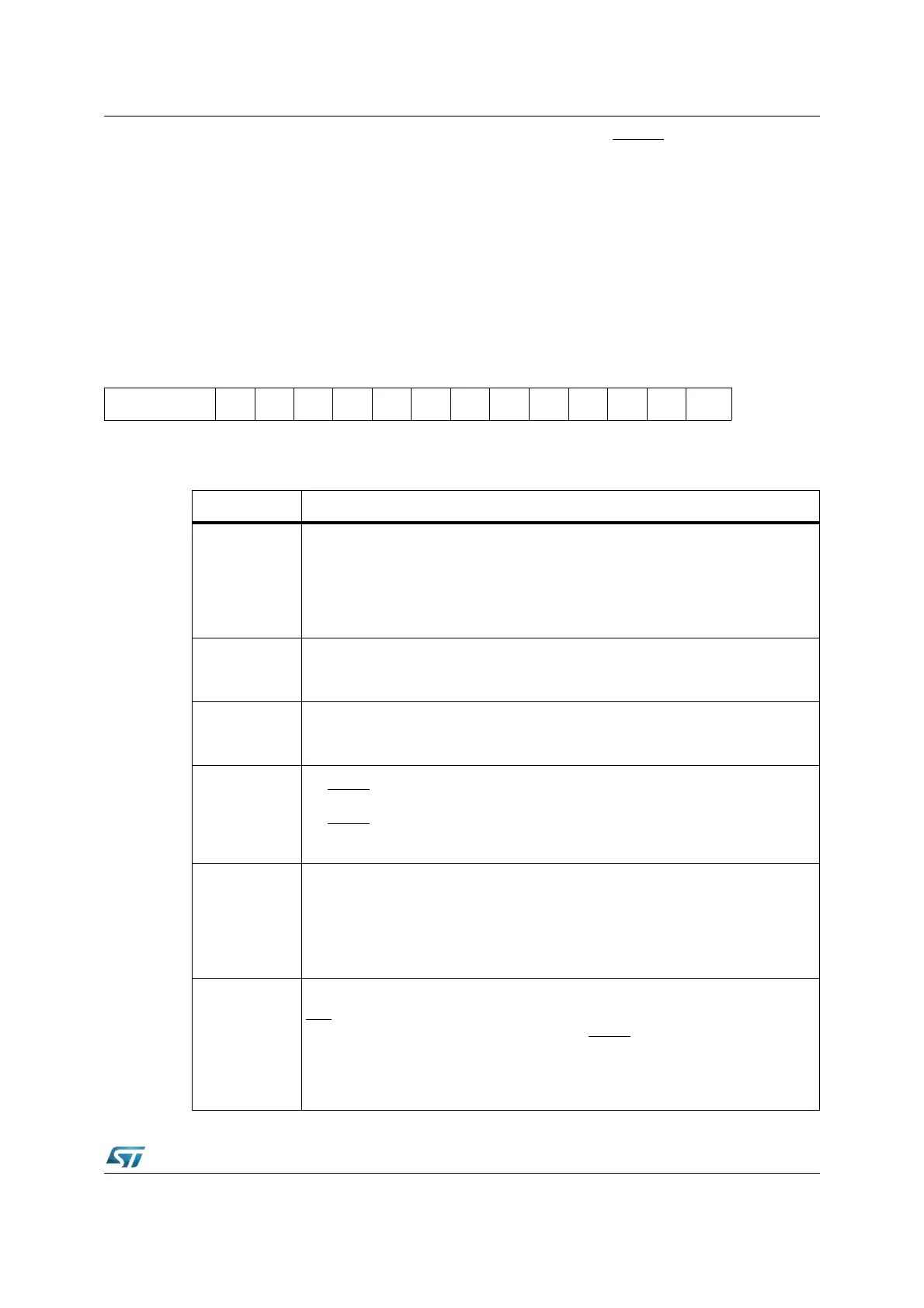
SYSCON (FF12h / 89h) SFR Reset Value: 0xx0h
Reset Value: 0000 0xx0 x000 0000b
15 14 13 12 11 10 9 8 7 6 5 4 3 2 1 0
STKSZ
ROM
S1
SGT
DIS
ROM
EN
BYT
DIS
CLK
EN
WR
CFG
CS
CFG
PWD
CFG
OWD
DIS
BDR
STEN
XPEN
VISI
BLE
XPER-
SHARE
RW RW RW
RW RW RW RW RW RW RW RW RW RW RW
Bit Function
XPER-SHARE
XBUS Peripheral Share Mode Control
‘0’: External accesses to XBUS peripherals are disabled.
‘1’: XRAM1 and XRAM2 are accessible via the external bus during hold mode.
External accesses to the other XBUS peripherals are not guaranteed in terms of
AC timings. See Section 2.4.1: XRAM access via external masters on page 50 for
additional details.
VISIBLE
Visible Mode Control
‘0’: Accesses to XBUS peripherals are done internally.
‘1’: XBUS peripheral accesses are made visible on the external pins.
XPEN
XBUS Peripheral Enable bit
‘0’: Accesses to the on-chip X-peripherals and XRAM are disabled.
‘1’: The on-chip X-peripherals are enabled.
BDRSTEN
Bidirectional Reset Enable
‘0’: RSTIN
pin is an input pin only. SW Reset or WDT Reset have no effect on this
pin.
‘1’: RSTIN
pin is a bidirectional pin. This pin is pulled low during internal reset
sequence.
OWDDIS
Oscillator Watchdog Disable Control
‘0’: Oscillator Watchdog (OWD) is enabled. If PLL is bypassed, the OWD monitors
XTAL1 activity. If there is no activity on XTAL1 for at least 1 μs, the CPU clock is
switched automatically to PLL’s base frequency (from 750 kHz to 3 MHz).
‘1’: OWD is disabled. If the PLL is bypassed, the CPU clock is always driven by
XTAL1 signal. The PLL is turned off to reduce power supply current.
PWDCFG
Power Down Mode Configuration Control
‘0’: Power Down Mode can only be entered during PWRDN instruction execution if
NMI pin is low, otherwise the instruction has no effect. To exit Power Down Mode,
an external reset must occur by asserting the RSTIN
pin.
‘1’: Power Down Mode can only be entered during PWRDN instruction execution if
all enabled fast external interrupt EXxIN pins are in their inactive level. Exiting this
mode can be done by asserting one enabled EXxIN pin or with external reset.