The external bus interface UM0404
198/564 DocID13284 Rev 2
The layout of the five BUSCON registers is identical. Registers BUSCON4...BUSCON1,
which control the selected address windows, are completely under software control, while
register BUSCON0, which is also used for the very first code access after reset, is partly
controlled by hardware, and it is initialized via PORT0 during the reset sequence.
This hardware control allows to define an appropriate external bus for systems, where no
internal program memory is provided.
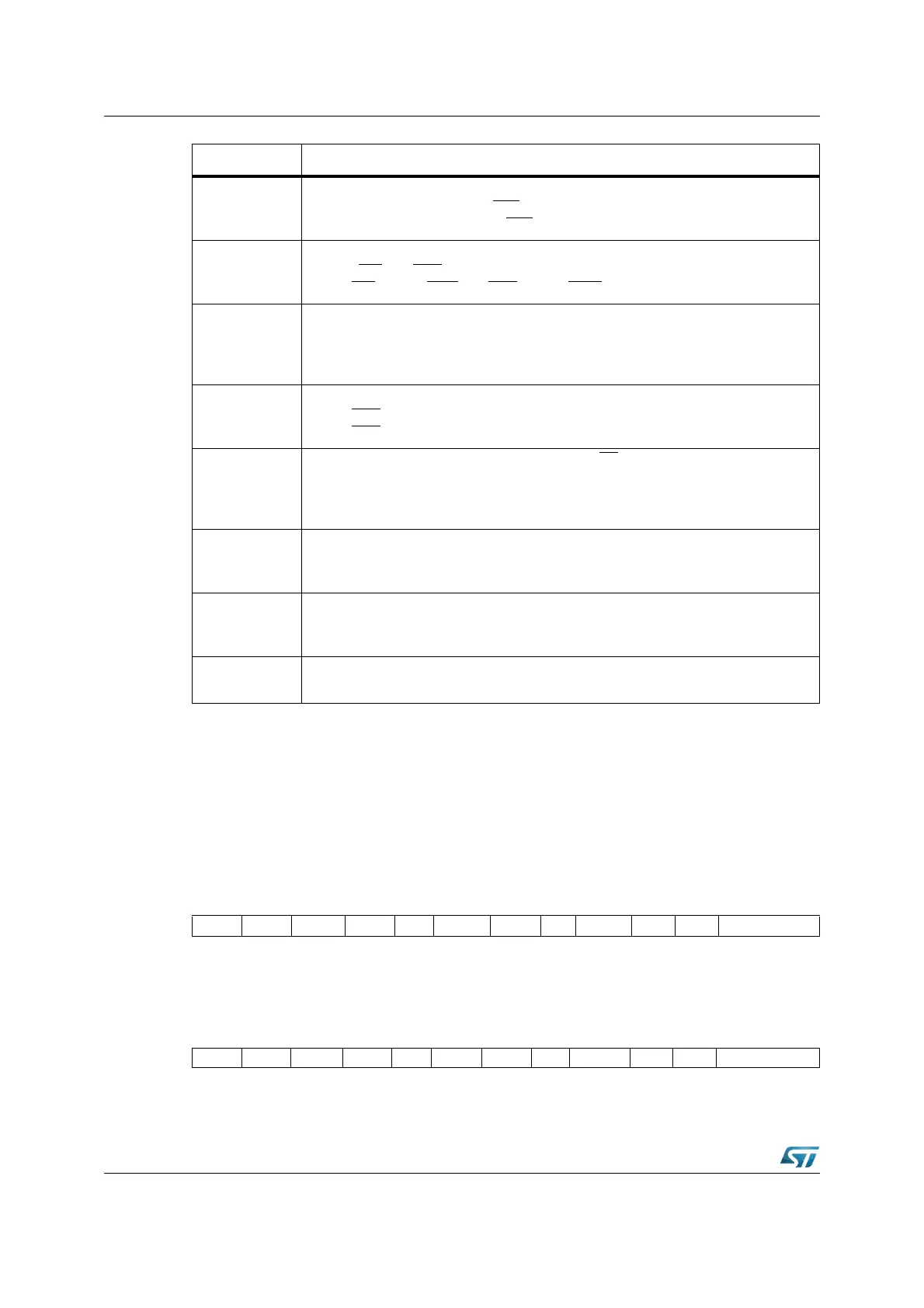
BUSCON0 (FF0Ch / 86h) SFR Reset Value: 0xx0h
BUSCON0 Reset Value: 0000 0xx0 xx00 0000b
BUSCON1 (FF14h / 8Ah) SFR Reset Value: 0000h
CSCFG
Chip Select Configuration Control
‘0’: Latched Chip Select lines, CSx changes 1 TCL after rising edge of ALE.
‘1’: Unlatched Chip Select lines, CSx
changes with rising edge of ALE.
WRCFG
Write Configuration Control (Inverted copy of WRC bit of RP0H)
‘0’: Pins WR
and BHE retain their normal function.
‘1’: Pin WR
acts as WRL, pin BHE acts as WRH.
CLKEN
System Clock Output Enable (CLKOUT)
‘0’: CLKOUT disabled, pin may be used for general purpose I/O.
‘1’: CLKOUT enabled, pin outputs the system clock signal or a prescaled value of
system clock according to XCLKOUTDIV register setting.
BYTDIS
Disable/Enable Control for Pin BHE (Set according to data bus width)
‘0’: Pin BHE
enabled.
‘1’: Pin BHE
disabled, pin may be used for general purpose I/O.
ROMEN
Internal Memory Enable (Set according to pin EA
during reset)
‘0’: Internal memory disabled: accesses to the IFlash Memory area use the
external bus.
‘1’: Internal memory enabled.
SGTDIS
Segmentation Disable/Enable Control
‘0’: Segmentation enabled (CSP is saved/restored during interrupt entry/exit).
‘1’: Segmentation disabled (Only IP is saved/restored).
ROMS1
Internal Memory Mapping
‘0’: Internal memory area mapped to segment 0 (00’0000h...00’7FFFh).
‘1’: Internal memory area mapped to segment 1 (01’0000h...01’7FFFh).
STKSZ
System Stack Size
Selects the size of the system stack (in the IRAM) from 32 to 1024 words.
15 14 13 12 11 10 9 8 7 6 5 4 3 2 1 0
CSWEN0 CSREN0 RDYPOL0 RDYEN0 - BUSACT0 ALECTL0 - BTYP MTTC0 RWDC0 MCTC
RW RW RW RW RW RW RW RW RW
15 14 13 12 11 10 9 8 7 6 5 4 3 2 1 0
CSWEN1 CSREN1 RDYPOL1 RDYEN1 - BUSACT1 ALECTL1 - BTYP MTTC1 RWDC1 MCTC
RW RW RW RW RW RW RW RW RW RW
Bit Function