DocID13284 Rev 2 199/564
UM0404 The external bus interface
BUSCON2 (FF16h / 8Bh) SFR Reset Value: 0000h
BUSCON3 (FF18h / 8Ch) SFR Reset Value: 0000h
BUSCON4 (FF1Ah / 8Dh) SFR Reset Value: 0000h
15 14 13 12 11 10 9 8 7 6 5 4 3 2 1 0
CSWEN2 CSREN2 RDYPOL2 RDYEN2 - BUSACT2 ALECTL2 - BTYP MTTC2 RWDC2 MCTC
RW RW RW RW RW RW RW RW RW
15 14 13 12 11 10 9 8 7 6 5 4 3 2 1 0
CSWEN3 CSREN3 RDYPOL3 RDYEN3 - BUSACT3 ALECTL3 - BTYP MTTC3 RWDC3 MCTC
RW RW RW RW RW RW RW RW RW
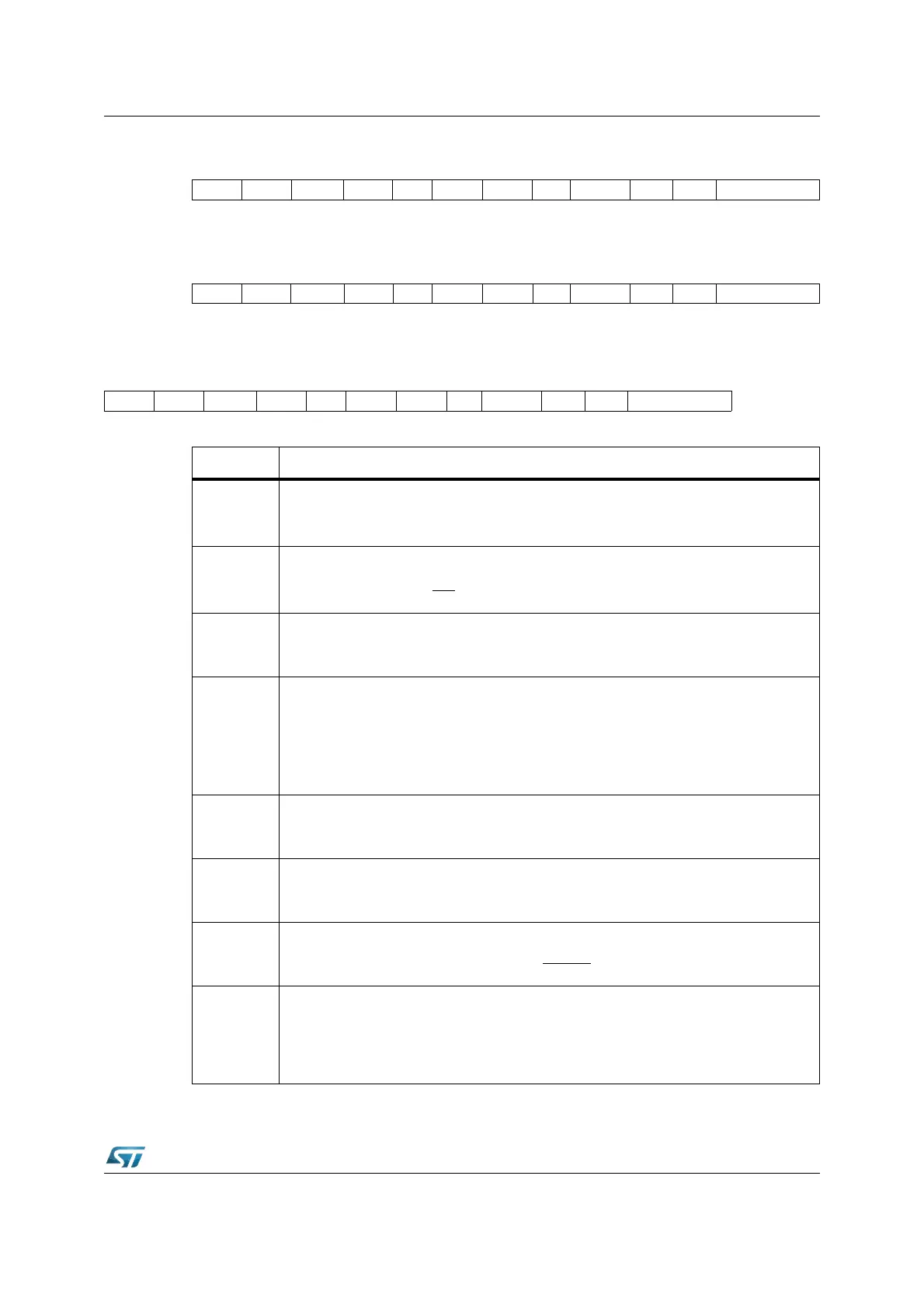
15 14 13 12 11 10 9 8 7 6 5 4 3 2 1 0
CSWEN4 CSREN4 RDYPOL4 RDYEN4 - BUSACT4 ALECTL4 - BTYP MTìTC4 RWDC4 MCTC
RW RW RW RW RW RW RW RW RW
Bit Function
MCTC
Memory Cycle Time Control (Number of memory cycle time wait-states)
‘0000’: 15 wait-states (Number of wait-states = 15 - [MCTC]).
‘1111’: No wait-states.
RWDCx
Read/Write Delay Control for BUSCONx
‘0’: With read/write delay, the CPU inserts 1 TCL after falling edge of ALE.
‘1’: No read/write delay, RW
is activated after falling edge of ALE.
MTTCx
Memory Tristate Time Control
‘0’: 1 wait-state.
‘1’: No wait-state.
BTYP
External Bus Configuration
‘00’: 8-bit De-multiplexed Bus
‘01’: 8-bit Multiplexed Bus
‘10’: 16-bit De-multiplexed Bus
‘11’: 16-bit Multiplexed Bus
Note: For BUSCON0 BTYP is defined via PORT0 during reset.
ALECTLx
ALE Lengthening Control
‘0’: Normal ALE signal.
‘1’: Lengthened ALE signal.
BUSACTx
Bus Active Control
‘0’: External bus disabled.
‘1’: External bus enabled (within the respective address window, see ADDRSEL).
RDYENx
READY Input Enable
‘0’: External bus cycle is controlled by bit field MCTC only.
‘1’: External bus cycle is controlled by the READY
input signal.
RDYPOLx
Ready Active Level Control
‘0’: Active level on the READY pin is low, bus cycle terminates with a ‘0’ on READY
pin.
‘1’: Active level on the READY pin is high, bus cycle terminates with a ‘1’ on READY
pin.