The external bus interface UM0404
200/564 DocID13284 Rev 2
Note: BUSCON0 is initialized with 0000h, if pin EA is high during reset. If pin EA is low during
reset, bit BUSACT0 and ALECTL0 are set (1) and bit-field BTYP is loaded with the bus
configuration selected via PORT0.
ADDRSEL1 (FE18h / 0Ch) SFR Reset Value: 0000h
ADDRSEL2 (FE1Ah / 0Dh) SFR Reset Value: 0000h
ADDRSEL3 (FE1Ch / 0Eh) SFR Reset Value: 0000h
ADDRSEL4 (FE1Eh / 0Fh) SFR Reset Value: 0000h
Note: Register BUSCON0 controls the complete external address space, except for the four
windows supported by BUSCON1 to BUSCON4, so there is no need of ADDRSEL0
register.
CSRENx
Read Chip Select Enable
‘0’: The CS signal is independent of the read command (RD).
‘1’: The CS
signal is generated for the duration of the read command.
CSWENx
Write Chip Select Enable
‘0’: The CS
signal is independent of the write command (WR, WRL, WRH).
‘1’: The CS
signal is generated for the duration of the write command.
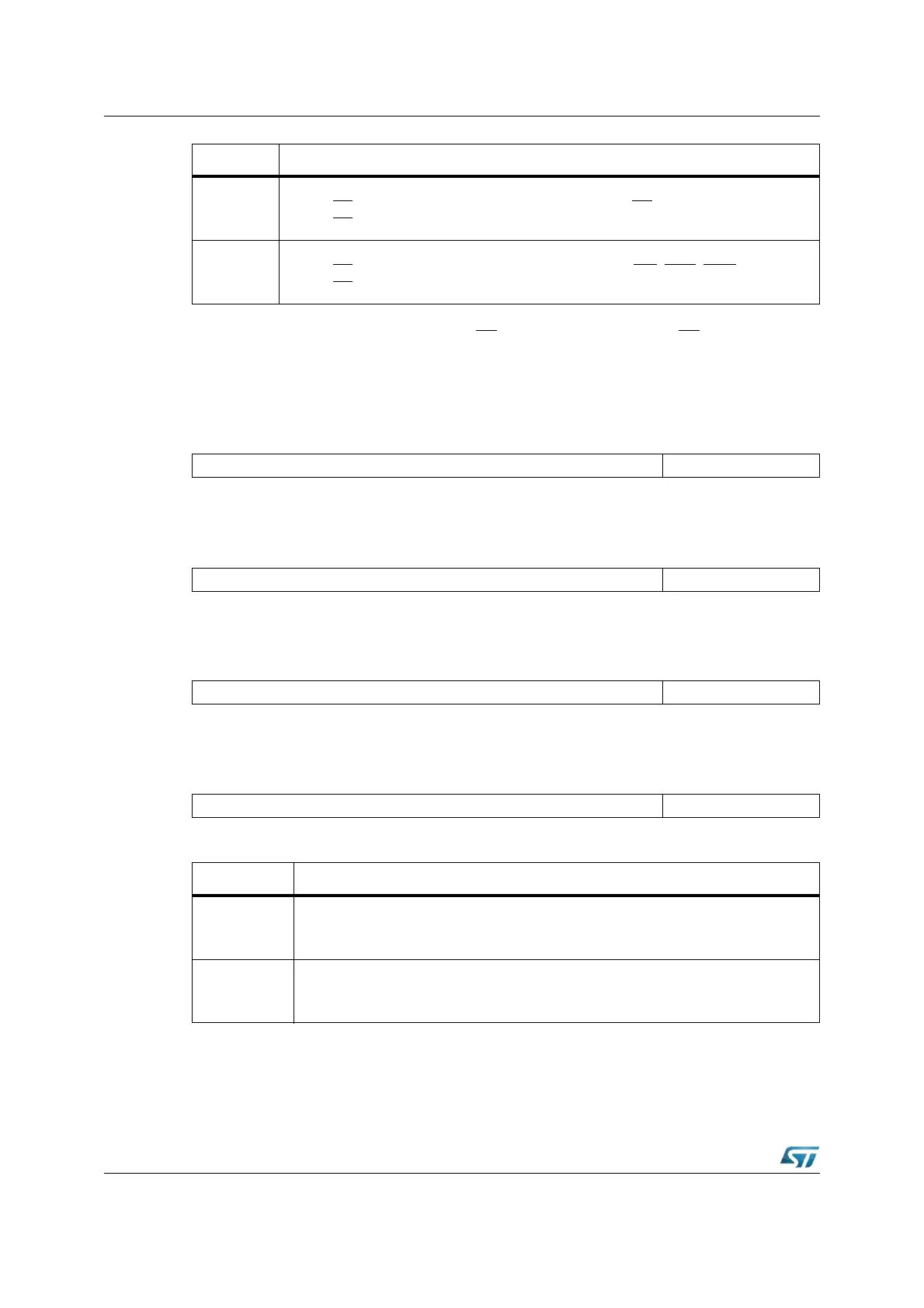
Bit Function
1514131211109876543210
RGSAD RGSZ
RW RW
1514131211109876543210
RGSAD RGSZ
RW RW
1514131211109876543210
RGSAD RGSZ
RW RW
1514131211109876543210
RGSAD RGSZ
RW RW
Bit Function
RGSZ
Range Size Selection
Defines the size of the address area controlled by the respective
BUSCONx/ADDRSELx register pair. See Table 30.
RGSAD
Range Start Address
Defines the upper bit of the start address (A23...) of the respective address area.
See Table 30.