System reset UM0404
498/564 DocID13284 Rev 2
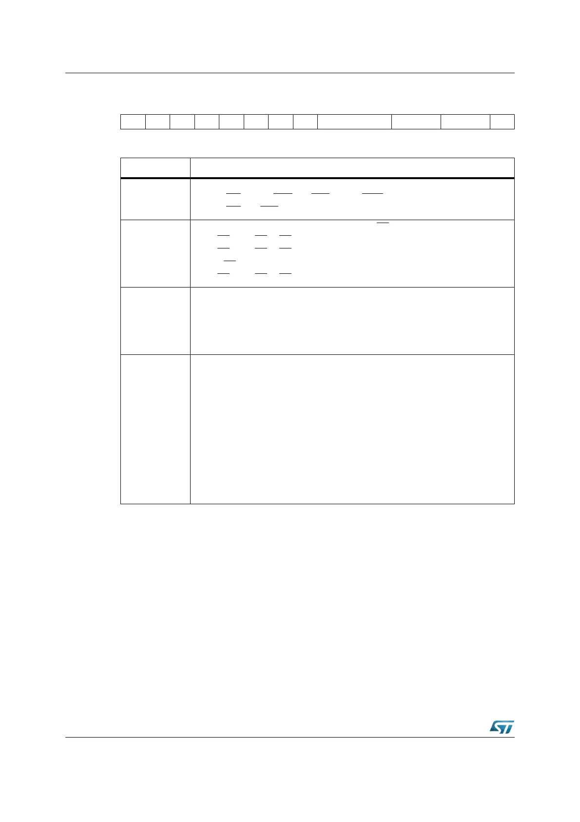
RP0H (F108h / 84h) SFR Reset Value: - - xxh
Pins controlling the operation of the internal logic and the reserved pins are evaluated only
during a hardware triggered reset sequence.
The pins that influence the configuration of the ST10F276 are evaluated during any reset
sequence, even during software and watchdog timer triggered resets.
The configuration via P0H is latched in register RP0H for subsequent evaluation by
software. Register RP0H is described in Section 8: The external bus interface on page 181.
Note: The reserved pins, P0L.2 and P0L.3, must remain high during reset in order to ensure
proper operation of the ST10F276. The load on those pins must be small enough for the
internal pull-up device to keep their level high, or external pull-up devices must ensure the
high level.
1514131211109876543210
- - - - - - - - CLKCFG SALSEL CSSEL WRC
R R
R
R
Bit Function
WRC
(1)
1. These bits are set according to Port0 configuration during any reset sequence.
Write Configuration Control
‘0’: Pins WR
acts as WRL, pin BHE acts as WRH
‘1’: Pins WR and BHE retain their normal function
CSSEL
(1)
Chip Select Line Selection (Number of active CS outputs)
0 0: 3 CS lines: CS2...CS0
0 1: 2 CS lines: CS1...CS0
1 0: No CS
lines at all
1 1: 5 CS lines: CS4...CS0 (Default without pull-downs)
SALSEL
(1)
Segment Address Line Selection (Number of active segment address outputs)
0 0: 4 Bit segment address: A19...A16
0 1: No segment address lines at all
1 0: 8 Bit segment address: A23...A16
1 1: 2 Bit segment address: A17...A16 (Default without pull-downs)
CLKCFG
(1)
(2)
2. RP0H.7 to RP0H.5 bits are loaded only during a long hardware reset. As pull-up resistors are active on
each Port P0H pins during reset, RP0H default value is ‘FFh’.
P0H.7-5 f
CPU
= f
XTAL
x F Notes
(3)
3. Refer to datasheet for more details about input clock ranges and limitations.
111 f
XTAL
x 4 Default configuration
110
f
XTAL
x 3
101
f
XTAL
x 8
100 f
XTAL
x 5
011
f
XTAL
Direct Drive (oscillator bypassed)
(3)
010 f
XTAL
x 10
001
f
XTAL
x 0.5 CPU clock via prescaler
(3)
000 f
XTAL
x 16