System reset UM0404
500/564 DocID13284 Rev 2
ST10F276 even for the first code fetch after reset. The two bits are copied into bit-field
BTYP of register BUSCON0. P0L.7 controls the data bus width, while P0L.6 controls the
address output (multiplexed or de-multiplexed). This bit-field may be changed via software
after reset, if required.
PORT0 and PORT1 are automatically switched to the selected bus mode. In multiplexed
bus modes PORT0 drives both the 16-bit intra-segment address and the output data, while
PORT1 remains in high impedance state as long as no de-multiplexed bus is selected via
one of the BUSCON registers. In de-multiplexed bus modes PORT1 drives the 16-bit intra-
segment address, while PORT0 or P0L (according to the selected data bus width) drives the
output data.
For a 16-bit data bus BHE
is automatically enabled, for an 8-bit data bus BHE is disabled via
bit BYTDIS in register SYSCON.
Default: 16-bit data bus with multiplexed addresses.
Note: If an internal start is selected via pin EA
, these two pins are disregarded and bit-field BTYP
of register BUSCON0 is cleared.
Write configuration: P0H.0
Pin P0H.0 (WRC) selects the initial operation of the control pins WR and BHE during reset.
When high, this pin selects the standard function, which is WR
control and BHE. When low,
it selects the alternate configuration, WRH
and WRL. Thus even the first access after a
reset can go to a memory controlled via WRH
and WRL. This bit is latched in register RP0H
and its inverted value is copied into bit WRCFG in register SYSCON.
Default: Standard function (WR
control and BHE).
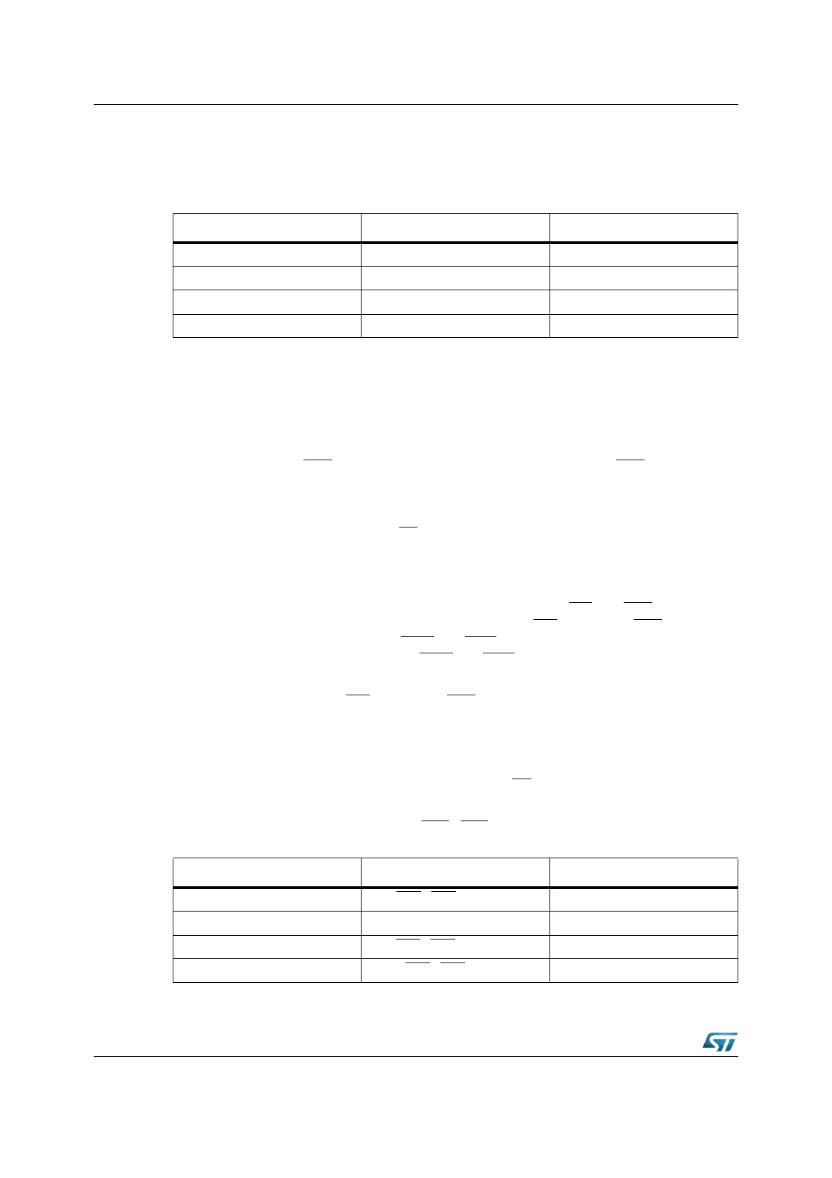
Chip select lines: P0H.1 - P0H.2
Pins P0H.2 and P0H.1 (CSSEL) define the number of active chip select signals during reset.
This allows to select which pins of Port6 drive external CS
signals and which are used for
general purpose I/O. The two bits are latched in register RP0H.
Default: All five chip select lines active (CS4
...CS0).
BTYP encoding External data bus width External address bus mode
0 0 8-bit Data De-multiplexed Addresses
0 1 8-bit Data Multiplexed Addresses
1 0 16-bit Data De-multiplexed Addresses
1 1 16-bit Data Multiplexed Addresses
CSSEL Chip Select Lines Note
1 1 Five: CS4
...CS0 Default without pull-downs
1 0 None Port6 pins free for I/O
0 1 Two: CS1
...CS0
0 0 Three: CS2...CS0