3-12
Cisco ONS 15454 DWDM Reference Manual, R8.5
78-18343-02
Chapter 3 Optical Service Channel Cards
3.4.1 Power Monitoring
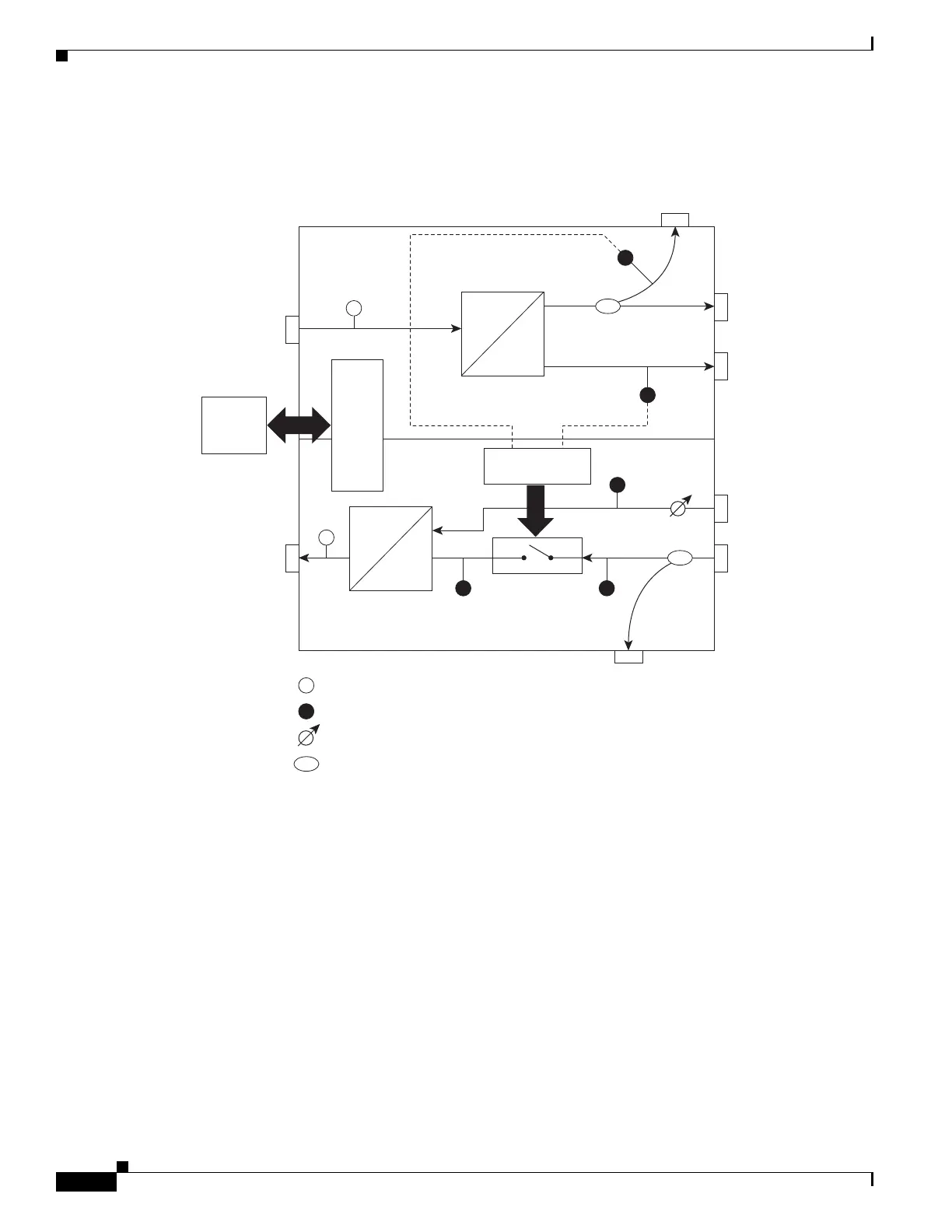
Figure 3-10 shows the OSC-CSM optical module functional block diagram.
Figure 3-10 OSC-CSM Optical Module Functional Block Diagram
3.4.1 Power Monitoring
Physical photodiodes P1, P2, P3, and P5 monitor the power for the OSC-CSM card. Their function is as
follows:
• P1 and P2: The returned power value is calibrated to the LINE RX port, including the insertion loss
of the previous filter (the reading of this power dynamic range has been brought backward towards
the LINE RX output).
• P3: The returned value is calibrated to the COM RX port.
• P5: The returned value is calibrated to the LINE TX port, including the insertion loss of the
subsequent filter.
The returned power level values are calibrated to the ports as shown in Table 3-5.
P P
P
P
P
V
V
124897
MON RX
MON TX
COM TX
OSC RX
COM RXLINE TX
LINE RX
DROP
section
ADD
section
OSC TX
Control
Interface
Filter
Filter
S1
P1
P2
P5
P4
PV1
PV2
P3
HW Switch
Control
Opt. Switch
S2
Virtual photodiode
Physical photodiode
Variable optical attenuator
P
V
Optical splitter
Control

 Loading...