7-47
Cisco ONS 15454 DWDM Reference Manual, R8.5
78-18343-02
Chapter 7 Reconfigurable Optical Add/Drop Cards
7.9.3 40-MUX-C Card Power Monitoring
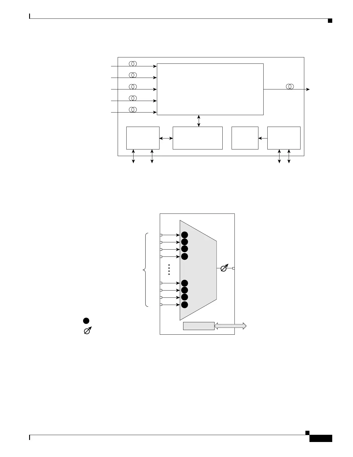
Figure 7-25 40-MUX-C Card Block Diagram
Figure 7-26 shows the 40-MUX-C optical module functional block diagram.
Figure 7-26 40-MUX-C Optical Module Functional Block Diagram
7.9.3 40-MUX-C Card Power Monitoring
Physical photodiodes P1 through P40 monitor the power of the individual input ports to the 40-MUX-C
card. P41 monitors the total multiplexed output power, calibrated to the COM-TX port. Table 7-26 shows
the returned power level values calibrated to each port.
Optical
module
36.6 to 42.1
8 CHS RX
30.3 to 35.8
8 CHS RX
42.9 to 48.5
8 CHS RX
49.3 to 54.9
8 CHS RX
55.7 to 61.4
8 CHS RX
Processor
COM TX
FPGA
For SCL Bus
management
SCL Bus
TCCi M
SCL Bus
TCCi P
DC/DC
Power supply
Input filters
BAT A&B
151974
1
40
Control
Control
interface
Physical photodiode
Variable optical attenuator
COM TX
Inputs
P40
P39
P38
P37
P4
P3
P2
P1
P
151975

 Loading...