6-22
Cisco ONS 15454 DWDM Reference Manual, R8.5
78-18343-02
Chapter 6 Optical Add/Drop Cards
6.6.1 Power Monitoring
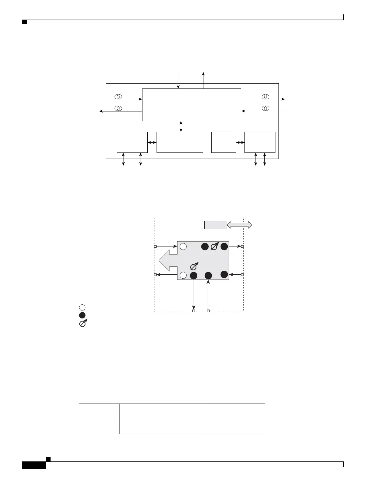
Figure 6-16 AD-1B-xx.x Block Diagram
Figure 6-17 shows the AD-1B-xx.x optical module functional block diagram.
Figure 6-17 AD-1B-xx.x Optical Module Functional Block Diagram
6.6.1 Power Monitoring
Physical photodiodes P1 through P4 and virtual photodiodes V1 and V2 monitor the power for the
AD-1B-xx.x card. The returned power level values are calibrated to the ports as shown in Table 6-15.
Optical
Module
COM RX
COM TX
124073
uP8260
processor
DC/DC
converter
EXP TX
EXP RX
FPGA
For SCL Bus
management
SCL Bus
TCC M
SCL Bus
TCC P
Power supply
Input filters
BAT A&B
Band xx.x
Rx
Band xx.x
Tx
98307
Control
Control
interface
Virtual photodiode
COM
RX
EXP
RX
EXP
TX
TX
Band xx.x
RX
Physical photodiode
Physical photodiode
V
V2
V1
COM
TX
P1
P3
P4P5
P2
P
Table 6-15 AD-1B-xx.x Port Calibration
Photodiode CTC Type Name Calibrated to Port
P1 ADD BAND RX
P2 DROP BAND TX

 Loading...