4-8
Cisco ONS 15454 DWDM Reference Manual, R8.5
78-18343-02
Chapter 4 Optical Amplifier Cards
4.3.3 OPT-PRE Power Monitoring
Figure 4-7 OPT-PRE Block Diagram
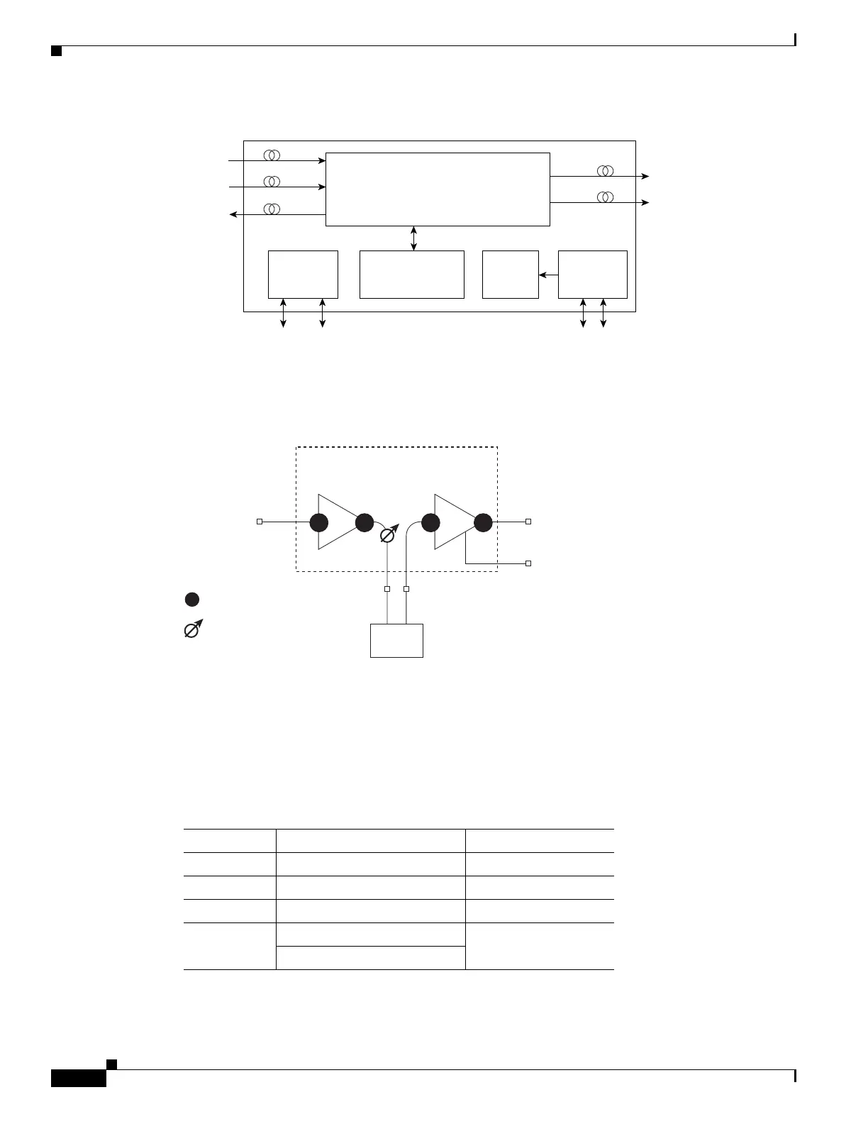
Figure 4-8 shows the a block diagram of how the OPT-PRE optical module functions.
Figure 4-8 OPT-PRE Optical Module Functional Block Diagram
4.3.3 OPT-PRE Power Monitoring
Physical photodiodes P1, P2, P3, and P4 monitor the power for the OPT-PRE card. Table 4-3 shows the
returned power level values calibrated to each port.
Optical
module
COM RX
DC RX
96478
Processor
DC TX
COM TX
MON
FPGA
For SCL Bus
management
SCL Bus
TCCi M
SCL Bus
TCCi P
DC/DC
Power supply
Input filters
BAT A&B
98298
DCU
COM RX COM TX
DC RXDC TX
MON
P1 P2 P3 P4
P
Physical photodiode
Variable optical attenuator
Table 4-3 OPT-PRE Port Calibration
Photodiode CTC Type Name Calibrated to Port
P1 Input Com COM RX
P2 Output DC DC TX
P3 Input DC DC RX
P4 Output COM (Total Output) COM TX
Output COM (Signal Output)

 Loading...