CMS32L051 User Manual |Chapter 4 Clock Generation Circuit
www.mcu.com.cn 102 / 703
4.7.2 Register description
Table 4-10 is a list of registers used for the high-speed internal oscillation frequency correction
function.
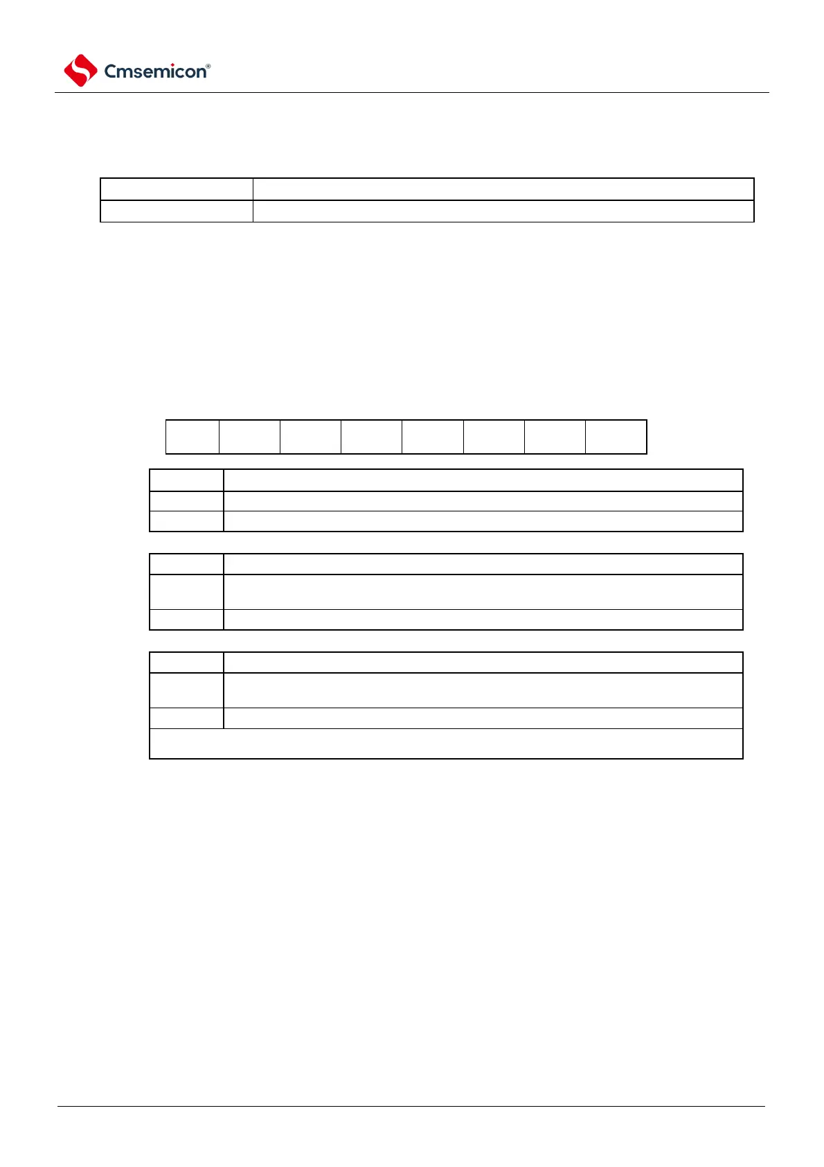
Table 4-10 Format of high-speed internal vibration frequency correction function registers
High Speed Internal Frequency Correction Control Register (HOCOFC)
4.7.2.1 High-speed internal oscillation frequency correction control register (HOCOFC).
Control register for high-speed internal oscillation frequency correction.
The HOCOFC register is set via an 8-bit memory operation command.
After the reset signal is generated, the value of this register becomes 00H.
Figure 4-19 Format of high-speed internal oscillation frequency correction control register (HOCOFC)
High-speed internal oscillation frequency correction function operation mode
Continuous operation mode
Interrupt control completed by high-speed internal oscillation frequency correction
There is no interruption after the high-speed internal oscillation frequency correction is
completed
Interrupts occur after high-speed internal oscillation frequency correction is complete
High speed internal frequency correction circuit motion control/status
The high-speed internal oscillation frequency correction circuit is in the process of
stopping/stopping
High-speed internal frequency correction circuit operation starts/in motion
When in continuous operation mode, the software writes 0 to stop the action.
When the interval operation mode is complete, the hardware clears the FCST bit.
Note 1. When the FCST bit is 1, it is forbidden to override the FCMD bit.
2. When writing 1 to the FCST bit, first confirm that the value of the current FCST bit is 0 and
then write 1 to it. Since hardware clears priority, when writing 1 to the FCST bit immediately
after the interval operation is completed (when the interrupt generation is completed by high-
speed internal resonance frequency correction), the operation should be performed at least 1
cycle after the interrupt generation is completed after the high-speed internal resonance
frequency correction is completed.
After writing 0 to the FCST bit (the high-speed internal resonance frequency correction circuit
Operation stops), fHOCO prohibits writing 1 to the FCST bit for 2 cycles (the high-speed
internal resonance frequency correction circuit Operation begins).
Note: Bit 5 to 1 must be written to 0.