CMS32L051 User Manual |Chapter 11 A/D Converter
www.mcu.com.cn 281 / 703
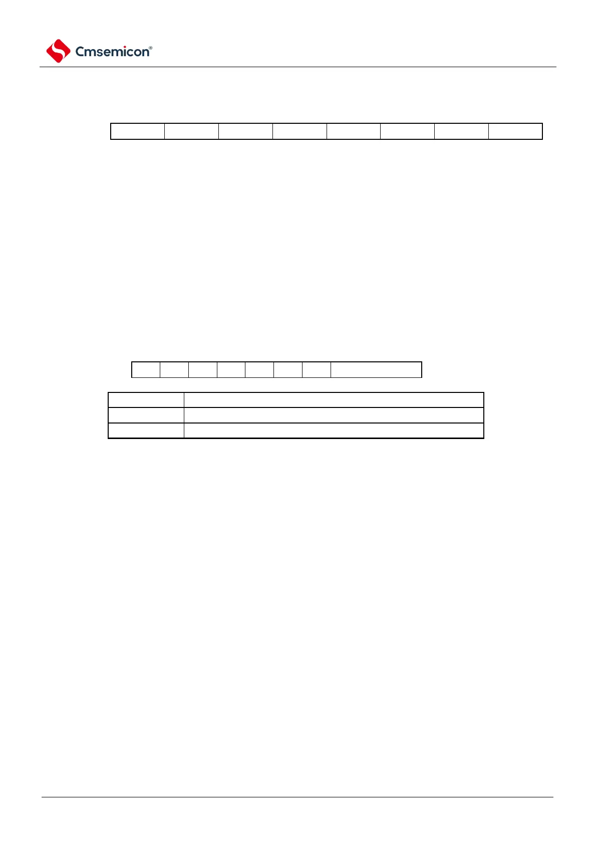
Figure11-13 Format of Conversion result comparison lower limit setting register (ADLL)
Note 1 Only the 12-bit A/D is converted to the high 8-bit and ADUL registers of the result register (ADCR) and the ADLL
Registers are compared.
2. To override the ADUL register and the ADLL register, it must be done in the transition stop state (ADCS=0).
3. When setting the ADUL register and the ADLL register, the ADUL must be > ADLL.
11.2.11 A/D converter sampling time extension control register (ADSMPWAIT)
This register is used to extend the A/D sampling time.
The ADSMPWAIT register is set via an 8-bit memory operation command.
After the reset signal is generated, the value of this register becomes 00H.
Figure11-14 Format of A/D converter sampling time extension control register (ADSMPWAIT)
When 0, the A/D sampling time is 4 ADCLKs
When 1, the A/D sampling time is 8 ADCLK
Note: Set ADSMPWAIT in the transition stop state (ADCS=0).
11.2.12 Registers for controlling the function of the analog input pin port
When using the ANIx pin as the analog input to an A/D converter, the port must be configured as an
analog channel by setting the corresponding Port Mode Control Register (PMCxx) bit to 1. For details,
please refer to Chapter 2 Pin Functions.