CMS32L051 User Manual |Chapter 14 Serial interface IICA
www.mcu.com.cn 499 / 703
14.4 Function of I
2
C-bus mode
14.4.1 Pin structure
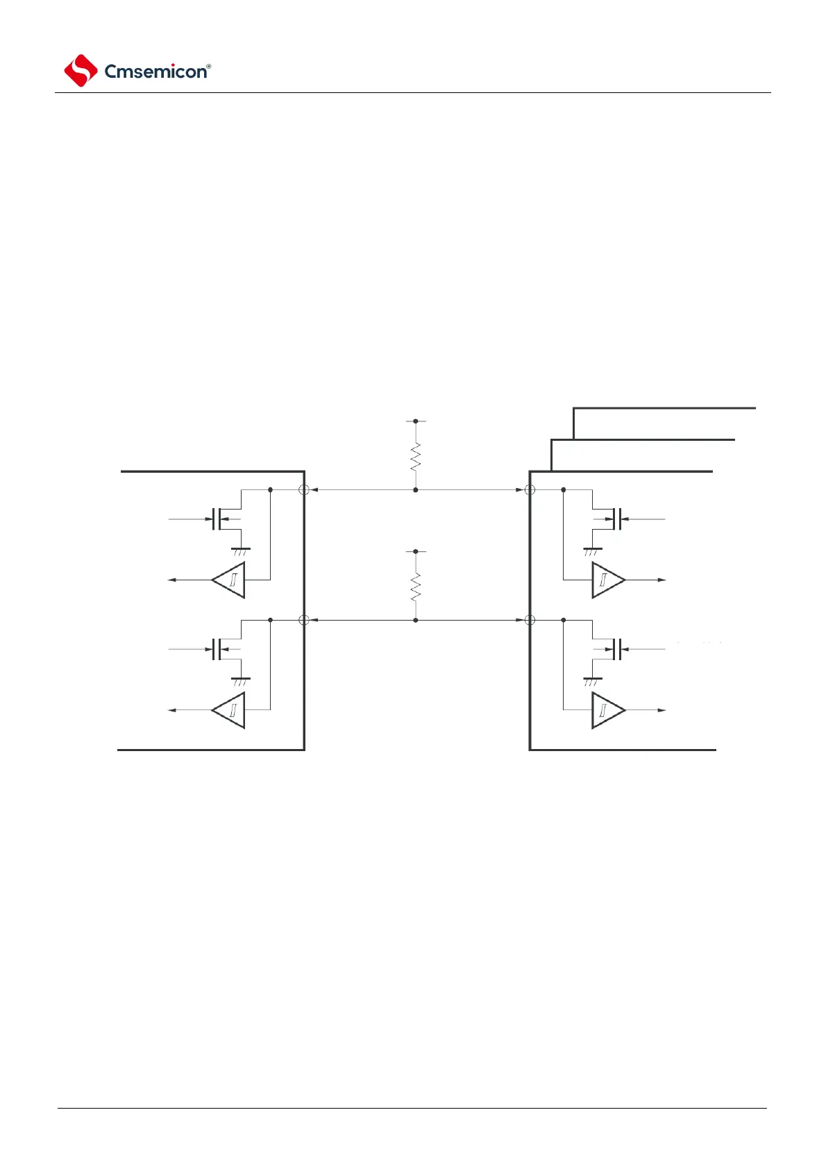
The structure of the serial clock pin (SCLAn) and the serial data bus pin (SDAAn) is as follows.
(1) SCLAn...... input/output pin of the serial clock
The outputs of the master and slave devices are N-channel open-drain outputs, and the inputs are
Schmitt inputs.
(2) SDAAn...... input/output multiplexing pin for serial data
The outputs of the master and slave devices are N-channel open-drain outputs, and the inputs are
Schmitt inputs.
Because the outputs of the serial clock line and serial data bus are N-channel open-drain outputs, an
external pull-up resistor is required.
Figure 14-12 Pin structure diagram