CMS32L051 User Manual |Chapter 4 Clock Generation Circuit
www.mcu.com.cn 67 / 703
4.3.2 System clock control register (CKC)
This is the register that selects the CPU/peripheral hardware clock and the main system clock.
The CKC register is set via an 8-bit memory operation instruction.
After the reset signal is generated, the value of this register becomes 00H.
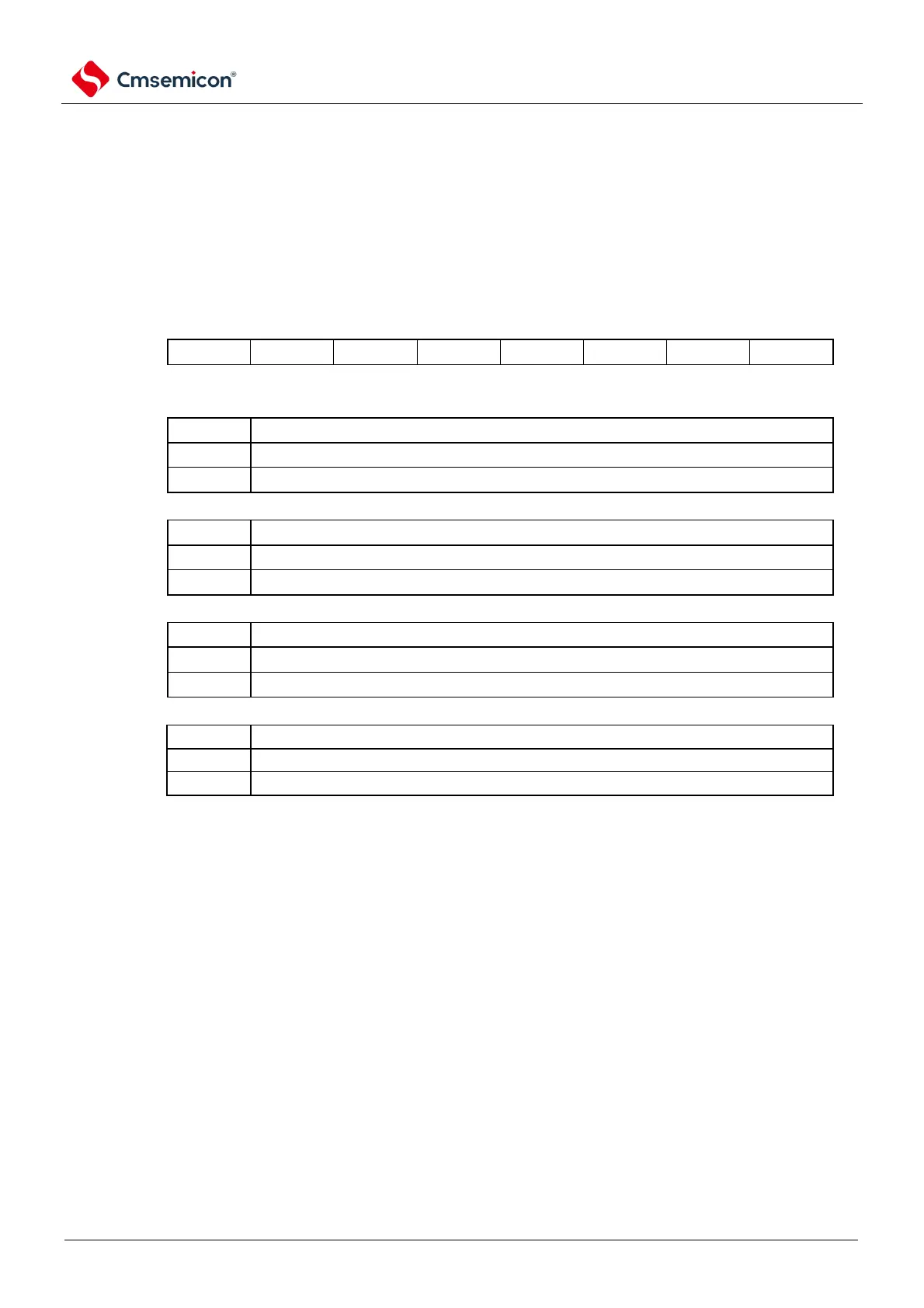
Figure 4-3 Format of system clock control register (CKC)
Address: 40020404H After reset: 00H R/W
Note
1
Symbol
7 6 5 4 3 2 1 0
CKC
Note 1. Bit7 and bit5 are read-only bits.
2. It is forbidden to change the value of the MCM0 bit in the state of placing the CSS position 1.
Note f
HOCO:
The clock frequency of a high-speed internal oscillator
f
IH
: The clock frequency of a high-speed internal oscillator
f
MX:
High-speed system clock frequency
f
MAIN:
Main system clock frequency
f
SUB:
Subsystem clock frequency
Note 1 You must set bit0~3 to 0.
2. Provide a clock for CSS bit settings for the CPU and peripheral hardware. If you change the CPU clock, you change
the clocks of the peripheral hardware at the same time (except for the real-time clock, the 15-bit interval timer, the
clock output/buzzer output, and the watchdog timer). Therefore, if you want to change the clock of the
CPU/peripheral hardware, you must stop each peripheral function.
3. If the subsystem clock is used as the peripheral hardware clock, the operation of the A/D converter and IICA cannot
be guaranteed. For the operating characteristics of peripheral hardware, please refer to the chapters and data
sheets of each peripheral hardware.