CMS32L051 User Manual |Chapter 5 Universal Timer Unit (Timer4)
www.mcu.com.cn 133 / 703
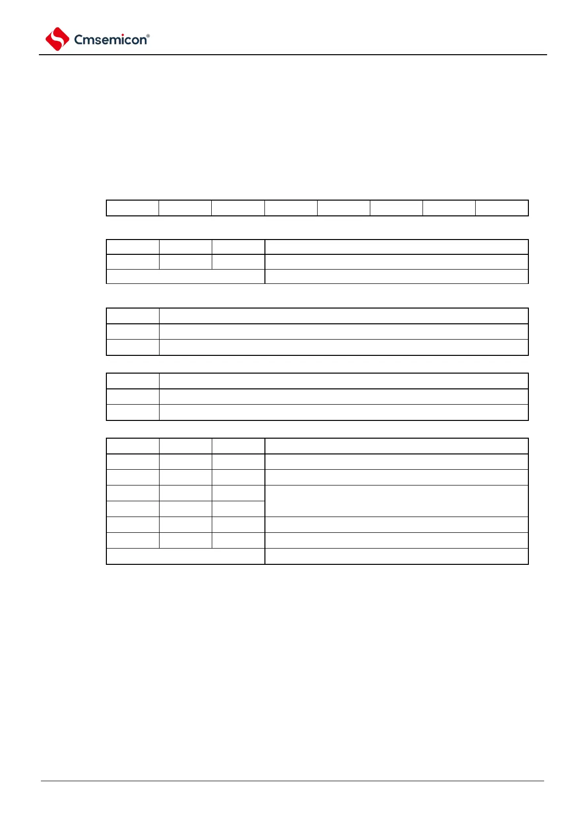
5.3.8 Timer input-output select register (TIOS0)
The TIOS0 register is used to select the input and output of unit 0. Select the timer inputs for Channel
0 and Channel 1 of Unit 0 and the timer output for Channel 2. The TIOS0 register is set via an 8-bit
memory operation command. After the reset signal is generated, the value of the TIOS0 register changes
to 00H.
Figure 5-17 Table of timer input selection register 0 (TIOS0)
Symbol
7 6 5 4 3 2 1 0
TIOS0
Channel 0 uses the selection of timer inputs
The input signal of the timer input pin (TI00).
Channel 0 uses the selection of timer inputs
Input signal selected via TIS07~TIS05
The event input signal for ELC
Enable of the timer output of channel 2
Disable output (output fixed at 0).
Channel 1 uses the selection of timer inputs
The input signal of the timer input pin (TI01).
The event input signal for ELC
The input signal of the timer input pin (TI01).
Low-speed internal oscillator clock (f
IL
).
Note 1 The high or low level width of the selected timer input needs to be greater than or equal to 1/fMCK+10ns.
Therefore, when selecting fSUB as fCLK (CSS=1 for CKC registers), TIS02 position 1 cannot be used.
2. When selecting the event input signal of ELC by timer input Register 0 (TIOS0), it must be selected by timer clock
selection register 0 (TPS0). fCLK.