CMS32L051 User Manual |Chapter 12 Universal Serial Communication Unit
www.mcu.com.cn 320 / 703
12.3.12 Serial output register m (SOm)
The SOm register is a buffer register for the serial output of each channel.
The value of the SOmn bit of this register is output from the serial data output pin of channel n.
The value of the CKOmn bit of this register is output from the serial clock output pin of channel n.
The SOmn bit of this register can only be rewritten by software when serial output is disabled
(SOEmn=0). When serial output (SOEmn=1) is allowed, the value of the SOmn bit of this register can only be
changed by serial communication by software overwriting.
The CKOmn bit of this register can only be rewritten by software only when the channel is stopped
(SEmn=0). When allowing the channel to run (SEmn=1), the value of the CKOmn bit of this register can only
be changed by serial communication by overriding the software.
To use the serial interface pins for non-serial interface functions such as port functions, the corresponding
CKOmn bit and SOmn bit must be set to "1".
The SOm register is set via a 16-bit memory operation command.
After the reset signal is generated, the value of the SOm register changes to 0F0FH.
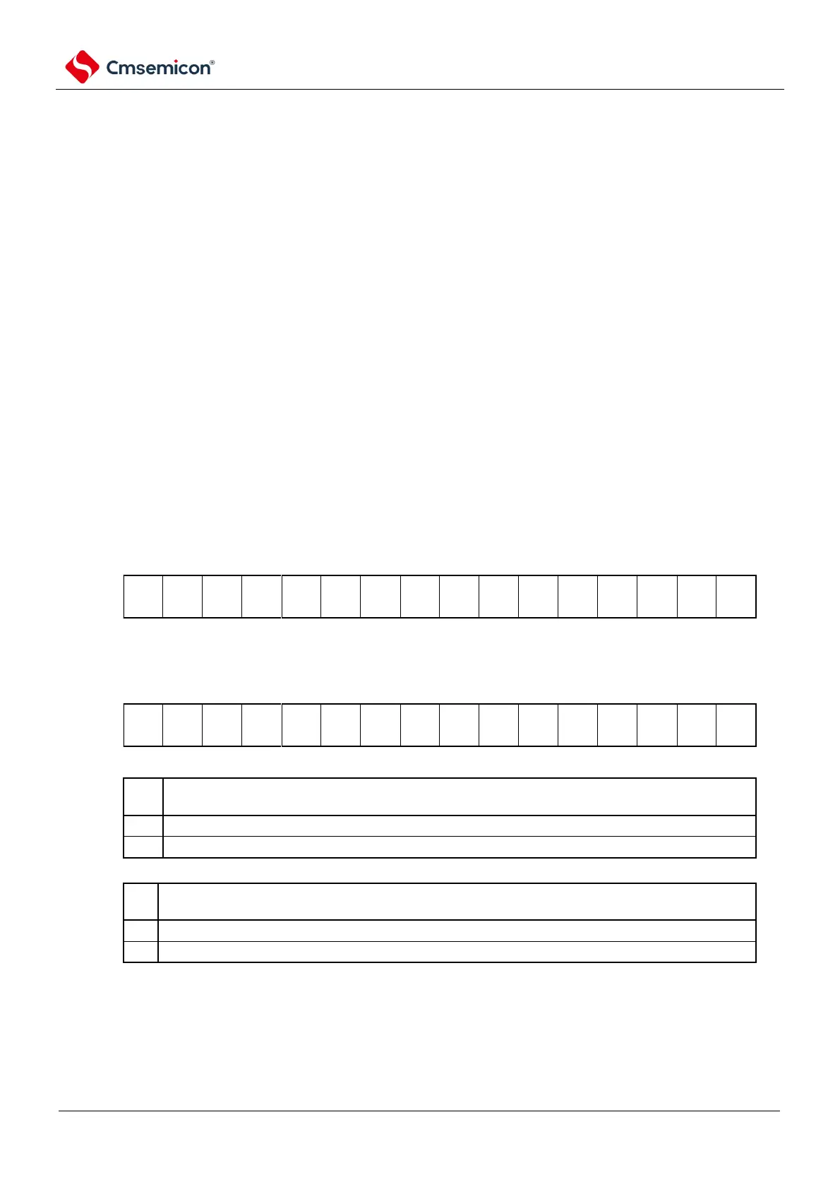
Figure 12-16 Format of serial output register m (SOm)
Address: 40041128H After reset: 0F0FHR/W
Symbol
15 14 13 12 11 10 9 8 7 6 5 4 3 2 1
0
SO0
Address: 40041568H After reset: 0303HR/W
Symbol
15 14 13 12 11 10 9 8 7 6 5 4 3 2 1
0
SO1
Note Bit15~12 and bit7~4 of the SO0 register must be set to 0.
Bit15~10 and bit7~2 of the SO1 register must be set to 0.
Notice m: unit number (m=0, 1) n: channel number (n=0~3).