CMS32L051 User Manual |Chapter 12 Universal Serial Communication Unit
www.mcu.com.cn 299 / 703
12.2 Structure of universal serial communication unit
The universal serial communication unit consists of the following hardware.
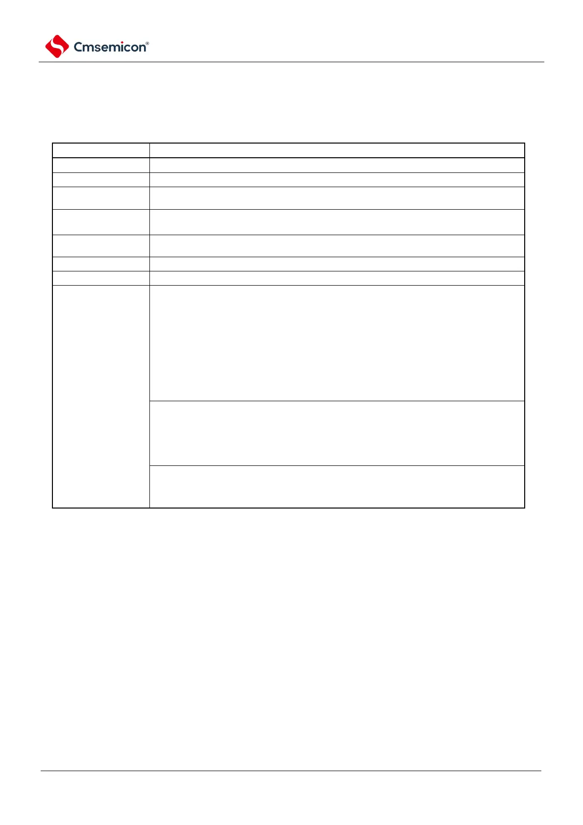
Table 12-1 Structure of universal serial communication unit
The serial data register mn (SDRmn) is 8 bits low or 9 bits
Note
1
and
2
Serial clock input/output
SCLK00, SCLK01, SCLK10, SCLK11, SCLK20, SCLK21 pins (for 3-wire serial I/O).
SCL00, SCL01, SCL10, SCL11, SCL20, SCL21 pins (for Easy I
2
C)
SDI00, SDI01, SDI10, SDI11, SDI20, SDI21 pins (for 3-wire serial I/O),
RxD0, RxD1, RxD2 pins (for UART).
SDO00, SDO01, SDO10, SDO11, SDO20, SDO21 pins (for 3-wire serial I/O),
TxD0, TxD1, TxD2 pins (for UART).
SDA00, SDA01, SDA10, SDA11, SDA20, SDA21 pins (for Simplified I
2
C)
SS00 pin (for slave select input function).
< Register of Unit Setting Section >
0 (PER0).
m (SPSm).
enable status register m (SEm).
m (SSm).
m (STm).
m (SOEm).
m (SOm).
m (SOLm).
switch control register (ISC).
enable register 0 (NFEN0).
< register for each channel >
mn (SDRmn).
mn (SMRmn).
operation setting register mn (SCRmn).
mn (SSRmn).
mn (SIRmn).
Port multiplexing function configuration register (PxxCFG).
output mode register (POMxx).
Note 1 The number of bits used as shift registers and buffer registers varies by unit and channel.
= 00, 01: low 9-bit
Others: low 8-bit
2. Depending on the communication mode, the lower 8 bits of the serial data register mn (SDRmn) can be read and
written with the following SFR name.
SSPIp communication... SIOp (SSPIp Data Register).
UARTq receives... RXDq (UARTq Receive Data Register).
UARTq sends... TXDq (UARTq Transmit Data Register).
IICr Communications... SIOr (IICr Data Register).
Remark m: Unit number (m=0, 1) n: Channel number (n=0~3) p: SSPI number (p=00, 01, 10, 11, 20, 21)
q: UART number (q=0~2) r: IIC number (r=00, 01, 10, 11, 20, 21)