CMS32L051 User Manual |Chapter 16 Enhanced DMA
www.mcu.com.cn 599 / 703
16.4.4 Chain transfer
When the CHNE bit of the DMACRj(j=0~23) register is 1 (allow chain transfer), multiple data can be
transferred continuously through one startup source.
Once the DMA is started, the control data is selected by reading the data from the corresponding vector
address of the startup source, and the control data assigned to the DMA control data area is read. If the CHNE
bit of the read control data is 1 (allowing chain transfer), the transfer continues after the transfer is completed
by reading the next assigned control data. Repeat this operation until the control data transfer with the CHNE
bit 0 (disable chain transmission) ends.
When multiple control data are used for chain transfer, the number of transmissions set by the first control
data is valid, while the number of transmissions of the control data processed after the second is invalid.
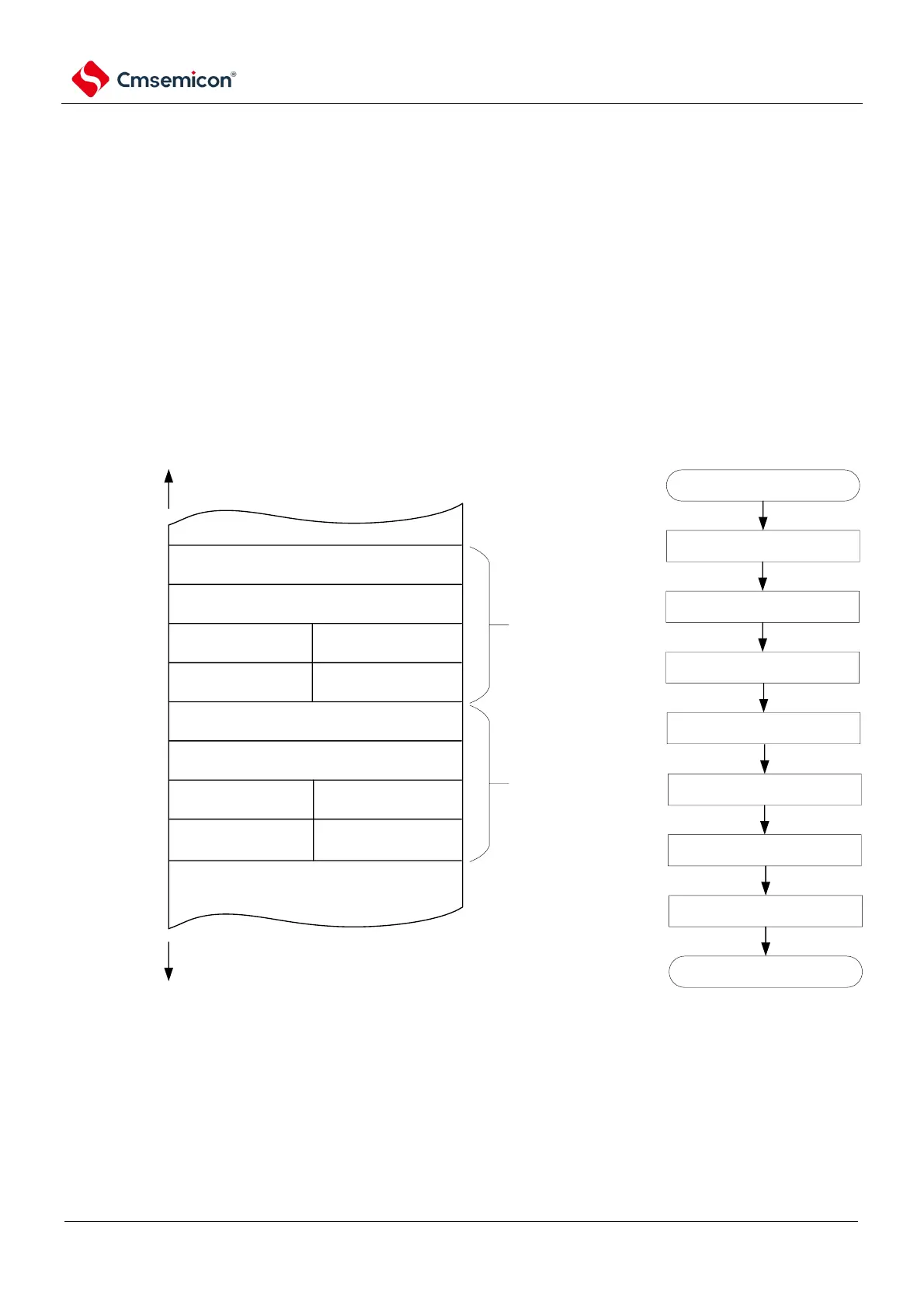
The flowchart of chain transfer is shown in Figure 16-20.
Figure 16-20 Flow chart of chain transfers
DMDAR2 register
DMSAR2 register
DMRLD2 register DMACT2 register
DMBLS2 register DMACR2 register
DMDAR1 register
DMSAR1 register
DMRLD1 register DMACT1 register
DMBLS1 register DMACR1 register
higher address bits lower address bits
00000000H
FFFFFFFFH
control data 2
(CHNE bit is "0")
control data 1
(CHNE bit is "1")
DMA trigger source occurs
read vector
read control data 1
transmit data
write back control data 1
read control data 2
transmit data
write back control data 2
DMA transfer completes
Note 1. The CHNE bit of the DMACR23 register must be 0 (chain transfer is prohibited).
2. In the data transfer after the second time of the chain transfer, the bits DMAENi0~DMAENi7 of DMAENi (i=0~2)
register does not change to 0 (DMA is prohibited from starting) and no interrupt requests are generated.