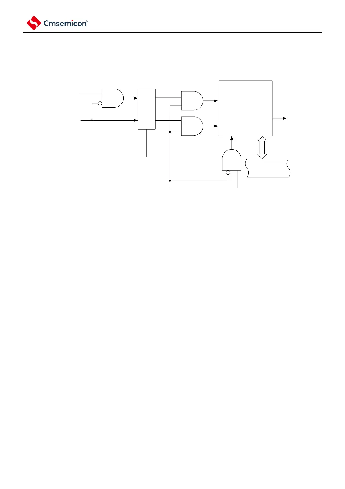
The following describes the output circuit of the Tomn pin.
(1) When the TOMmn bit is 0 (main channel output mode), ignore the timer output level register m
(TOLm) setting, and only INTTMmp (Slave Channel Timer Interrupt) passes the given timer output
register m (TOm).
(2) When the TOMmn bit is 1 (slave channel output mode), INTTMmn (master channel timer
interrupt) and INTTMmp (slave channel timer interrupt) are passed to the TOm register.
At this point, the TOLm register is valid and the following
signals are controlled:
TOLmn=0: Normal-phase operation (INTTMmn emset, INTTMmp reset)
TOLmn=1: Inverting operation (INTTMmn reset, INTTMmp set).
When both INTTMmn and INTTMmp (0% of the PWM output) are generated simultaneously, the
INTTMmn (reset signal) is preferred and the INTTMmn is masked (Set signal).
(3) In the state of allowing timer output (TOEmn=1), the INTTMmn (master channel timer interrupt)
and INTTMmp (slave channel timer interrupt) are passed to the TOm register. The write operation
of the TOm register (TOmn write signal) is invalid.
When the TOEmn bit is 1, the output of the TOmn pin is not changed except for the interrupt
signal.
To initialize the output level of the TOmn pin, the TOm register needs to be written after setting the
disable timer output (TOEmn=0).
(4) In the state of disabling the timer output (TOEmn=0), the write operation of the TOmn bit of the
object channel (TOmn write signal) is valid. When the timer output is in a disabled state
(TOEmn=0), INTTMmn (master channel timer interrupt) and INTTMmp (slave channel timer
interrupt) are not passed to the TOm register.
(5) The TOm register can be read at any time and the output level of the TOmn pin can be confirmed.
Remarks m: Unit number (m=0,1) n: channel number n=0~3 (master channel: n=0, 2 )
p: The slave channel number
n=0:p=1, 2, 3
n=2:p=3