EasyManua.ls Logo

Cmsemicon CMS32L051 - Port Register (Pxx)

Default Icon
703 pages
Print Icon
To Next Page IconTo Next Page
To Previous Page IconTo Previous Page
Loading...
V1.2.2
CMS32L051 User Manual |Chapter 2 Pin Function
www.mcu.com.cn 22 / 703
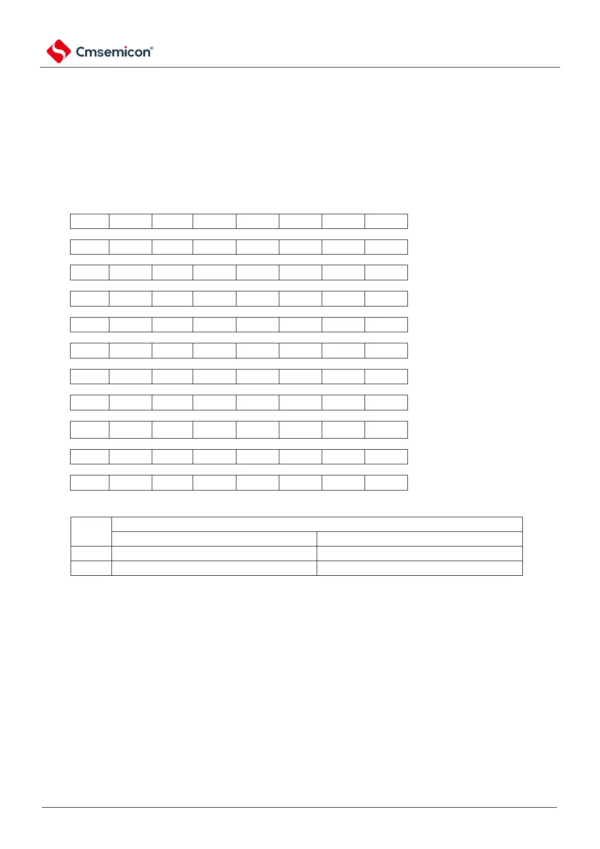
2.3.2 Port register (Pxx).
This is the register that sets the value of the port output latch in bits. Reading this register in input mode
gives the pin level, while reading it in output mode gives the value of the port's output latch. After the reset
signal is generated, the value of the register becomes 00H.
Register address = base address + offset address; the base address of the port register is 0x40040000,
and the offset address is shown in the following figure.
Figure 2-2 Format of port register
symbol
7
6
5
4
3
2
1
0
address
after reset
R/W
P0
0
0
0
0
0
0
P01
P00
0x000
00H (Output Latch).
R/W
P1
P17
P16
P15
P14
P13
P12
P11
P10
0x001
00H (Output Latch).
R/W
P2
P27
P26
P25
P24
P23
P22
P21
P20
0x002
00H (Output Latch).
R/W
P3
0
0
0
0
0
0
P31
P30
0x003
00H (Output Latch).
R/W
P4
0
0
0
0
0
0
P41
P40
0x004
00H (Output Latch).
R/W
P5
0
0
0
0
0
0
P51
P50
0x005
00H (Output Latch).
R/W
P6
0
0
0
0
P63
P62
P61
Note 2
P60
Note 2
0x006
00H (Output Latch).
R/W
P7
0
0
P75
P74
P73
P72
P71
P70
0x007
00H (Output Latch).
R/W
P12
0
0
0
P124
P123
P122
P121
P120
0x00C
00H (Output Latch).
R/W
P13
P137
P136
0
0
0
0
0
P130
0x00D
00H (Output Latch).
R/W
P14
P147
P146
0
0
0
0
0
P140
0x00E
00H (Output Latch).
R/W
Pmn
m=0~7, 12~1 4, n=0~7
Control of output data (output mode)
Reading of input data (input mode)
0
Output 0.
Input low level.
1
Output 1.
Input high level.
Note: 1. The initial value must be set for the unassigned bits.
2. It indicates that it is limited to CMS32L051xx-S series products only. When the products are not CMS32L051xx-S
series, ports P60 and P61 are dedicated N-channel open-drain output ports, which can only output 0 and Hiz .

Table of Contents

Related product manuals