CMS32L051 User Manual |Chapter 16 Enhanced DMA
www.mcu.com.cn 588 / 703
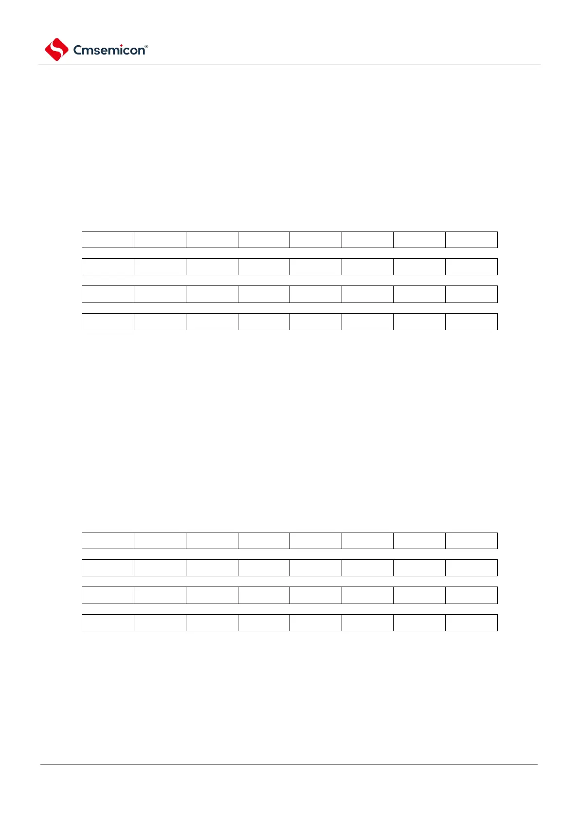
16.3.9 DMA source address register j(DMSARj) (j=0~23).
This register specifies the source address at which data is transferred.
When the SZ bit of the DMACRj register is 01 (16 bits transferred), the lowest bit is ignored and
processed as an even address.
When the SZ bit of the DMACRj register is 10 (32-bit transfer), the lower 2 bits are ignored and
processed as a word address.
Figure 16-10 Format of DMA source address register j (DMSARj)
Address:
Refer to 16.3.2
Control data allocation
.
After reset: Indefinite value
R/W
Note 1 The DMSARj register cannot be accessed via DMA transfer.
16.3.10 DMA destination address register j(DMDARj) (j=0~23).
This register specifies the destination address at which data is transferred.
When the SZ bit of the DMACRj register is 01 (16 bits transferred), the lowest bit is ignored and
processed as an even address.
When the SZ bit of the DMACRj register is 10 (32-bit transfer), the lower 2 bits are ignored and
processed as a word address.
Figure 16-11 format of the DMA destination address register j (DMDARj).
Address:
Refer to 16.3.2
Control data allocation
.
After reset: Indefinite value
R/W
Note: DMDARj registers cannot be accessed via DMA transfer.