CMS32L051 User Manual |Chapter 5 Universal Timer Unit (Timer4)
www.mcu.com.cn 112 / 703
5.2 Structure of the universal timer unit
The universal timer unit consists of the following hardware.
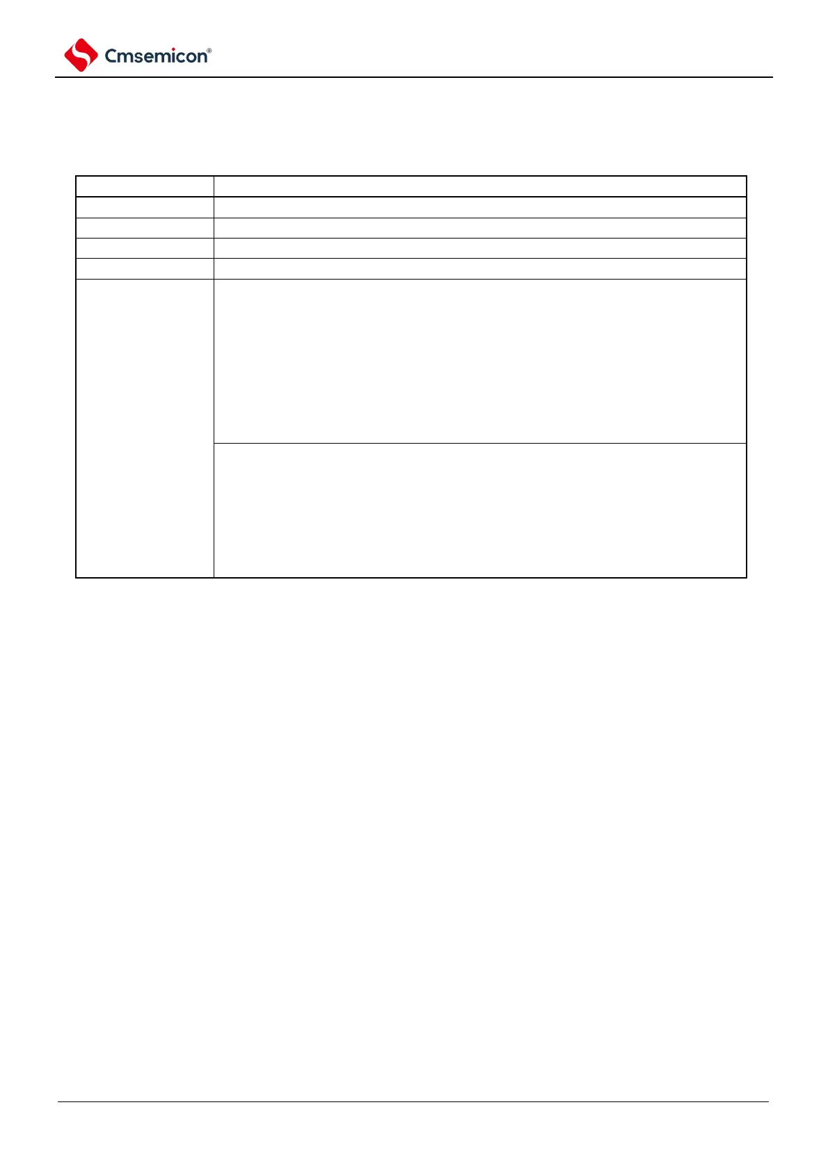
Table 5-1 Structure of the universal timer unit
Timer count register mn (TCRmn).
Timer data register mn (TDRmn).
TI00~TI03
Note
1
, TI10~TI13
Note
1
TO00~TO03
Note 1
, TO 1 0~TO13
Note 1
, Output control circuitry
< Unit setting register >
(PER0).
Timer clock selection register m (TPSm).
m (TEm).
m (TSm).
m (TTm).
0 (TIOS0)
Note 2
m (TOEm).
m (TOm).
m (TOLm).
m (TOMm).
< Each channel register >
mn (TMRmn).
mn (TSRmn).
1, 2 (NFEN1, NFEN2).
mode control register (PMCxx)
Note 3
mode register (PMxx)
Note 3
(PxxCFG)
Note 3
input multiplexing function configuration register (TI1XPCFG)
Note 3
Note 1: The input/output pins of general-purpose timer unit 0 are multiplexed to fixed ports, and the timer input/output
pins of channels 0 to 3 of general-purpose timer unit 1 can be arbitrarily configured to each port except RESETB.
For details, please refer to Chapter 2 Pin Functions.
Note 2: Channel selection for unit 0 only
Note 3: Timer input/output pin configuration for channels 0 to 3. For details, please refer to Chapter 2 Pin Functions.
Remark m: unit number (m=0,1) n: channel number (n=0~ 3).