CMS32L051 User Manual |Chapter 12 Universal Serial Communication Unit
www.mcu.com.cn 323 / 703
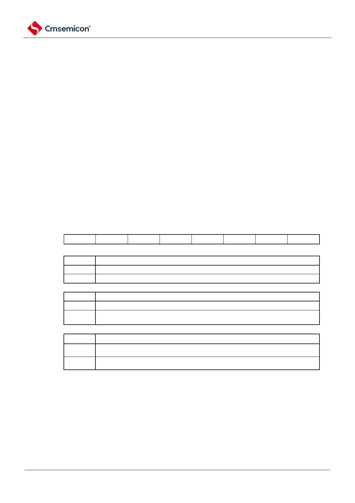
12.3.14 Input switching control register (ISC)
When implementing LIN-bus communication via UART0, the ISC1 and ISC0 bits of the ISC register are
used for the coordination of external interrupts and timer array units. If bit0 is set to 1, the input signal from
the serial data input (RxD0) pin is selected as the input for the external interrupt (INTP0) and therefore passes
The INTP0 interrupt detects the wake-up signal.
If bit1 is set to 1, the input signal from the serial data input (RxD0) pin is selected as the input to the timer,
so that the wake-up signal can be detected by the timer and the low-level width of the interval segment and the
pulse width of the synchronization segment can be measured.
The SS1E00 bit controls the SS00 pin input of channel 0 in slave mode of SSPI00 communication. During
the period when the SS00 pin is input high, no transmission and reception occurs even if the serial clock is input;
During the low input level to the SS00 pin, if a serial clock is entered, it is transmitted and received according to
the settings of each mode.
The ISC register is set via an 8-bit memory operation command.
After the reset signal is generated, the value of the ISC register changes to 00H.
Figure 12-19 Format of input switching control register (ISC)
Address: 40040473H After reset: 00HR/W
Symbol
7 6 5 4 3 2 1
0
ISC