2.5 Register setting when using the multiplexed function
2.5.1 Basic idea when using the multiplexed output feature
First, for analog pins, the port mode control register (PMCxx) sets whether the pin is used as an analog
function or as a digital input/output.
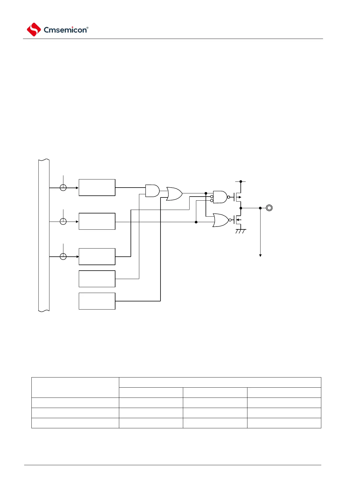
The basic structure of the output circuit when used as a digital input/output is shown in Figure 2. The output
of the SCI function that is multiplexed with the output latch output of the port is input to the AND gate, the output
of the AND gate is input to the OR gate, and the other input connections of the OR gate are multiplexed Output
of SCI functions (output of timer, RTC, clock/buzzer, IICA, etc.). When such a pin is used as a port function or
a multiplexed function, the unused multiplexing function cannot affect the output of the function to be used. The
basic idea of setting at this point is shown in Table 2-6.
Figure 2-14 Basic structure of pin output
GPIO/Concurrent function
Note: 1 When there is no POM register, this signal is Low level (0).
2. When there is no multiplexing function, this signal is High level (1).
3. When there is no multiplexing function, this signal is Low level (0).
Table 2-6 Basic principal of configuration
Note: Because it is possible to multiplex output functions other than multiple SCIs with one pin, the output of the unused
multiplexing function needs to be set to Low level (0). For details of the specific setting method, please refer to 2.5.2
Example of register settings using port functions and multiplexing functions.