CMS32L051 User Manual |Chapter 11 A/D Converter
www.mcu.com.cn 268 / 703
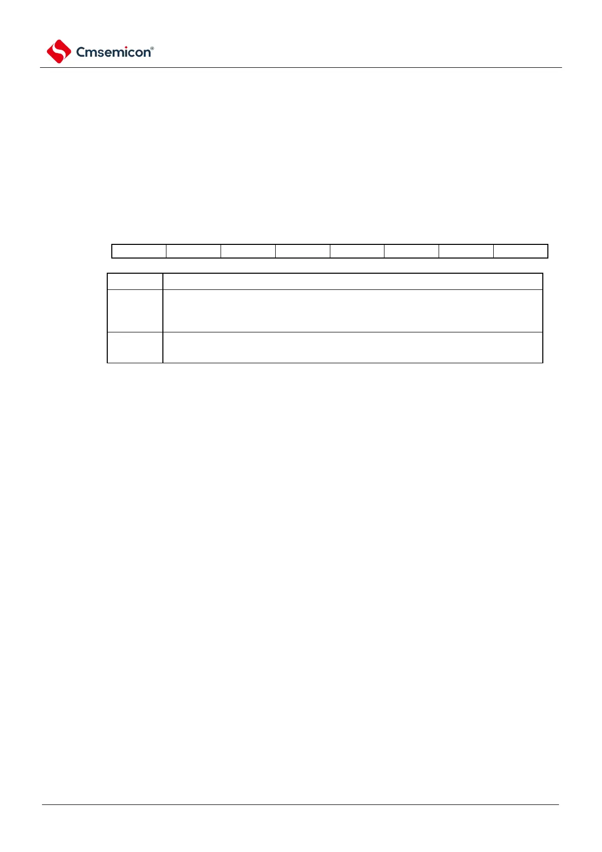
11.2.1 Peripheral enable register 0 (PER0)
The PER0 register is a register that sets the clock to be enable or disable to be supplied to each
peripheral hardware. Reduce power consumption and noise by stopping clocking unused hardware.
To use an A/D converter, bit5 (ADCEN) must be set to 1.
The PER0 register is set via an 8-bit memory operation command.
After the reset signal is generated, the value of this register becomes 00H.
Figure 11-2 Format of peripheral enable register 0 (PER0)
Control of the input clock of the A/D converter
Stop supplying the input clock.
A/D converters using SFR.
An input clock is provided.
to A/D converters used.
Note 1 To set up an A/D converter, you must first read and write the following registers in the ADCEN bit 1. When the
ADCEN bit is 0, the value of the control register of the A/D converter is the initial value, ignoring the write operation
(port mode control register (PMCxx except).
• A/D converter mode register 0 (ADM0)
• A/D converter mode register 1 (ADM1)
• A/D converter mode register 2 (ADM2)
• A/D converter trigger mode register (ADTRG)
• Analog input channel specification register (ADS)
• Conversion result comparison lower limit setting register (ADLL)
• Conversion result comparison upper limit setting register (ADUL)
• 12-bit A/D conversion result register (ADCR)
• 8-bit A/D conversion result register (ADCRH)
• A/D converter sampling time extension control register (ADSMPWAIT)