CMS32L051 User Manual | FLASH Control
www.mcu.com.cn 697 / 703
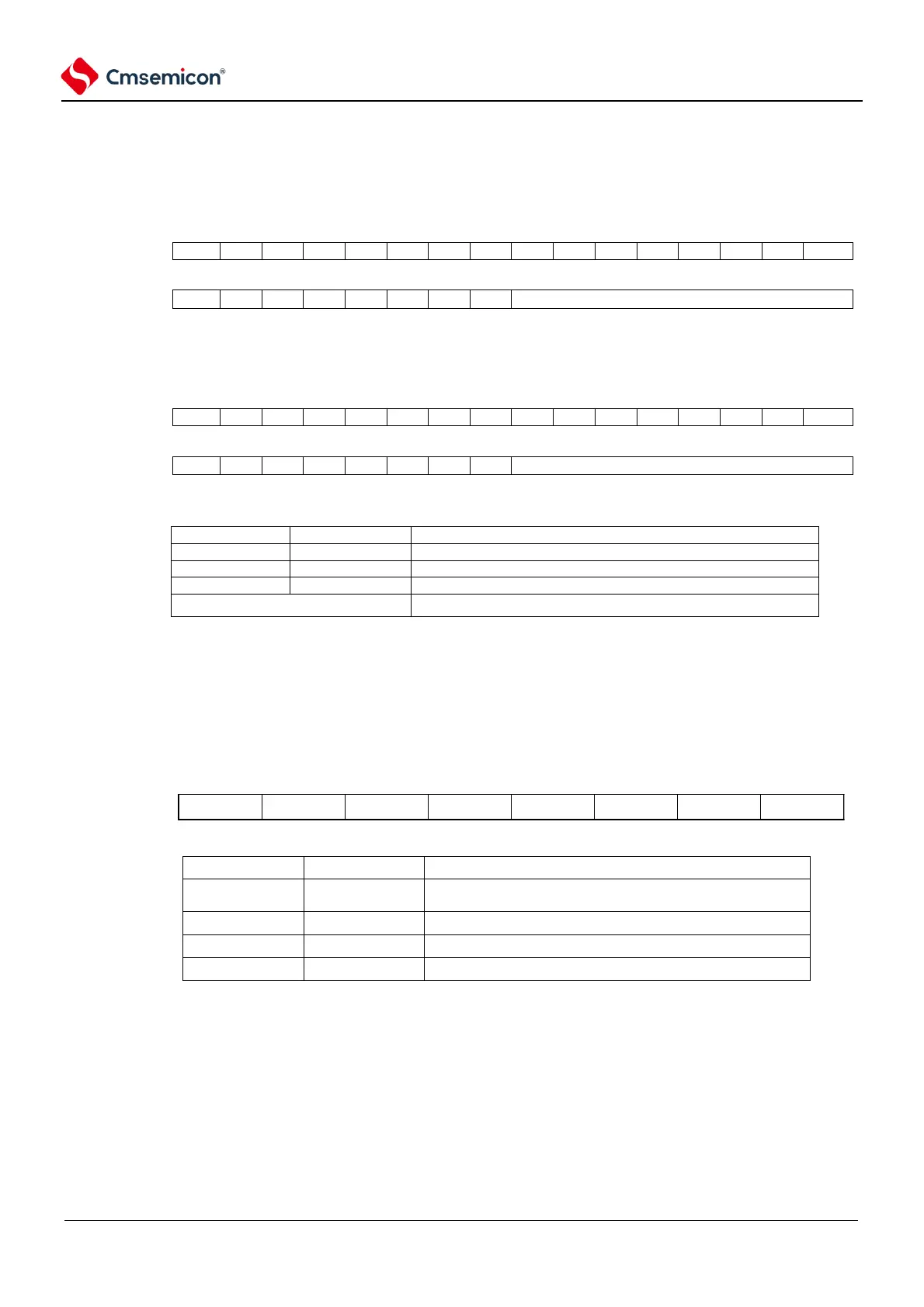
27.3.2 FLASH operation control registers (FLOPMD1, FLOPMD2)
Flash operation control registers for setting the erase and write operations of FLASH.
Address: 0x40020004 After reset: 000000000H R/W
symbol
FLOPMD1
Address: 0x40020008 after reset: 00HR/W
symbol
FLOPMD2
27.3.3 Flash erase control register (FLERMD)
Flash erasure control register to set the type of FLASH erase operation.
Address: 0x4002000C after reset: 00HR/W
Symbol
7 6 5 4 3 2 1 0
FLERMD
Note: chip wipe erases only the code flash area, not the data flash area. And chip erasure does not
support hardware verification.