CMS32L051 User Manual |Chapter 2 Pin Function
www.mcu.com.cn 33 / 703
2.3.10 Port input multiplexing function configuration registers (TI10PCFG, TI11PCFG, TI12PCFG,
TI13PCFG, INTP0PCFG, INTP1PCFG , INTP2PCFG, INTP3PCFG, SDI00PCFG,
SCLKI00PCFG, SS00PCFG , SDI20PCFG, SCLKI20PCFG, SDAA0PCFG, SCLA0PCFG,
RXD1PCFG )
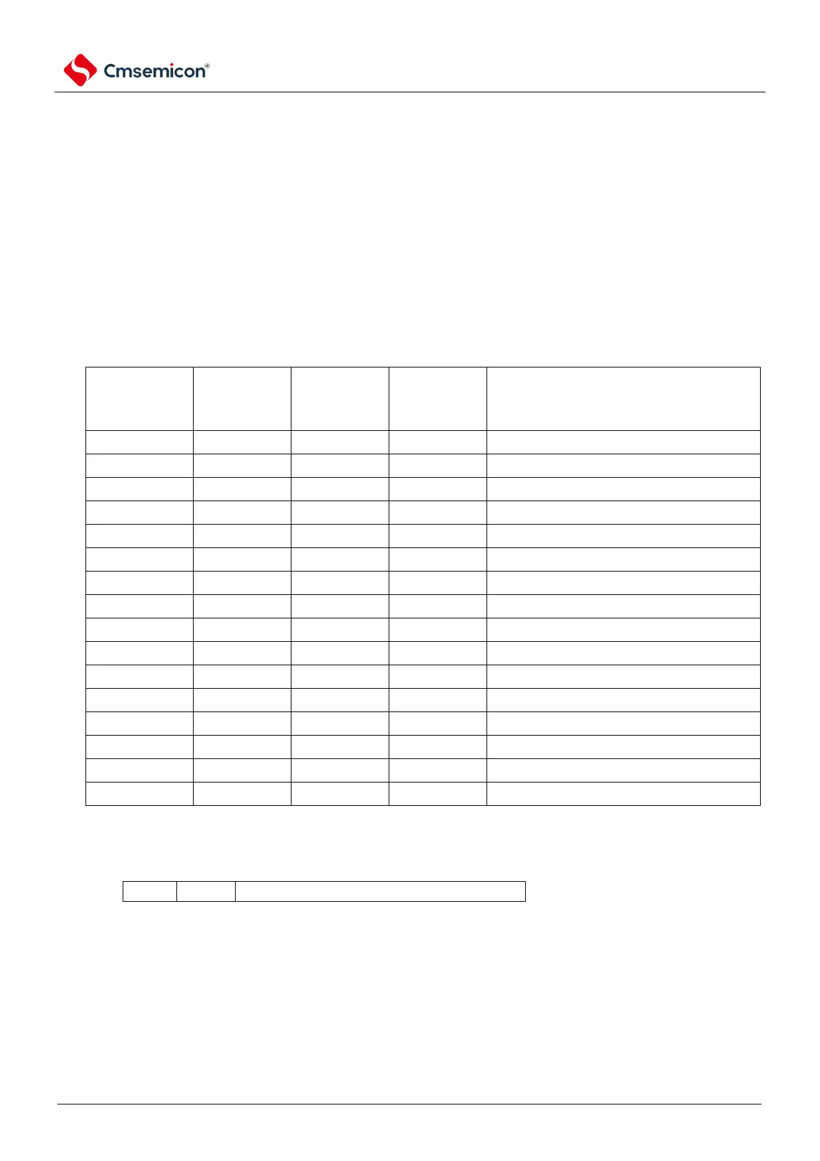
The Port Input Multiplexing Configuration Register enables the mapping of the input functions of
peripheral modules to individual ports. Reset Value of the port input multiplexing function configuration register
is 00H. 20 dual input functions (TI10, TI11, TI12, TI13, INTP0, INTP1, INTP2, INTP3, SDI00, RXD0, SDA00,
SCLKI00, SS00, SDI20, RXD2, IrRXD, SCLKI20, SDAA0, SCLA0, RXD1) maps to any port. Other than these
20 types of concurrent inputs can only be input from a fixed port.
Register address = base address + offset address; the base address of the register is 0x40040800, and
the offset address is shown in the following figure.
Figure 2-11 List of port input multiplexing function configuration registers