EasyManua.ls Logo

Cmsemicon CMS32L051 - SPI Port Multiplexing Configuration Register (SPIPCFG)

Default Icon
703 pages
Print Icon
To Next Page IconTo Next Page
To Previous Page IconTo Previous Page
Loading...
V1.2.2
CMS32L051 User Manual |Chapter 2 Pin Function
www.mcu.com.cn 37 / 703
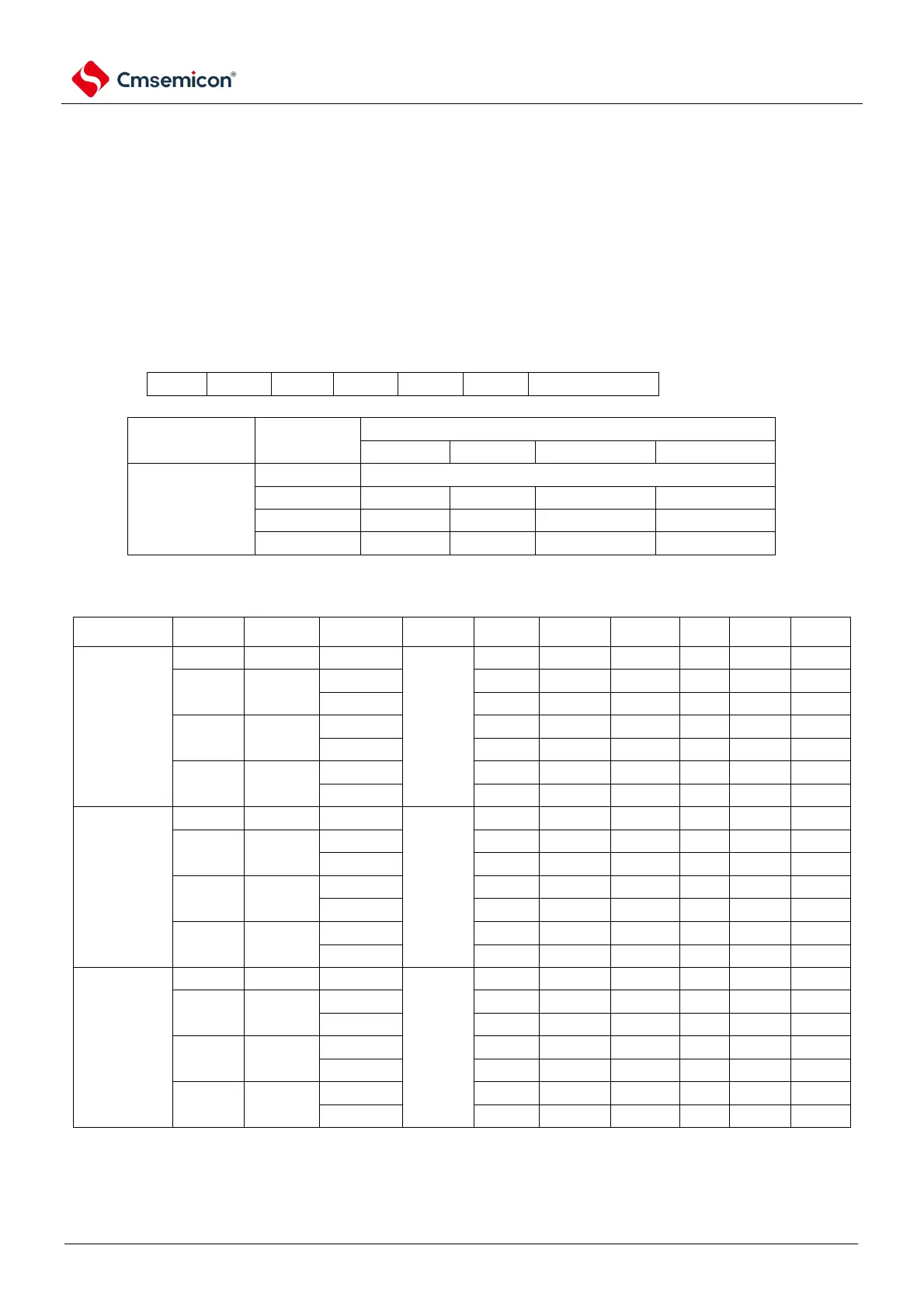
2.3.11 SPI port multiplexing configuration register (SPIPCFG)
The SPI Port multiplexing configuration register (SPIPCFG) enables the SPI communication function to be
mapped to three different sets of port combinations. The reset value of the SPI port multiplexing function
configuration register is 00H, and the SPI communication function is not mapped to any port.
Register address = base address + offset address; the base address of the SPIPCFG register is
0x40040800, and the offset address is shown in the figure below.
Figure 2-13 Format of port input multiplex configuration register
symbol
7
6
5
4
3
2
1
0
address
after reset
R/W
SPIPCFG
0
0
0
0
0
0
spipcfg[1:0]
0x07E
00H
R/W
The register name
Register
settings
Mapping relationships
NSS
SCK
MISO
MOSI
SPIPCFG[1:0]
2'b00
Does not map to any port
2'b01
P50
P51
P17
P16
2'b10
P63
P31
P75
P74
1'b11
P25
P24
P23
P22
Table 2-4 SPI communication port configuration method
SPI port
combination
Port
name
Function
name
Input/output
SPIPCFG
PxxCFP
xxPCFG
PMCxx
PMxx
POMxx
Pxx
spi_group1
P50
SPI_NSS
input

x
x
0
1
x
x
P51
SPI_SCK
output
x
x
0
0
0
0
input
x
x
0
1
x
x
P16
SPI_MOSI
output
x
x
0
0
0
0
input
x
x
0
1
x
x
P17
SPI_MISO
input
x
x
0
1
x
x
output
x
x
0
0
0
0
spi_group2
P63
SPI_NSS
input

x
x
0
1
x
x
P31
SPI_SCK
output
x
x
0
0
0
0
input
x
x
0
1
x
x
P74
SPI_MOSI
output
x
x
0
0
0
0
input
x
x
0
1
x
x
P75
SPI_MISO
input
x
x
0
1
x
x
output
x
x
0
0
0
0
spi_group3
P25
SPI_NSS
input

x
x
0
1
x
x
P24
SPI_SCK
output
x
x
0
0
0
0
input
x
x
0
1
x
x
P22
SPI_MOSI
output
x
x
0
0
0
0
input
x
x
0
1
x
x
P23
SPI_MISO
input
x
x
0
1
x
x
output
x
x
0
0
0
0

Table of Contents

Related product manuals